Is it important to understand the PCB fabrication and assembly process? Yes.
Though PCB fabrication and assembly is an outsourced work to your electronics contract manufacturer, it can affect the manufacturability of the project itself, the box-build assembly yield rate, and product lifespan or reliability.
This blog introduces the complete PCB fabrication and assembly process. Though PCBs of different substrate materials have differences in PCB fabrication and assembly, the PCB fabrication process is basically the same.
PCB fabrication and assembly at the electronic contract manufacturer strictly adhere to your specifications. So before the production, it is necessary to do the DFM (design for manufacturing) and PCB prototype to ensure your design is workable.
Now let's wait no more to see the manufacturer's factory's PCB fabrication and assembly process!
PCB Fabrication Process
Below is the PCB fabrication process of FR4 PCBs. This blog comprehensively covers all the PCBs, so the different points of MCPCB, PTFE PCB, flexible PCB, and ceramic PCB fabrication are also mentioned, in the notes.
PCB fabrication step 1. Cut laminate
PCB laminates are the materials for PCB fabrication. The first step is preparing the PCB materials, removing any oxidation layer or contamination, and sizing them into the required size for fabrication.
Because cutting is the most used method to size the laminates, we call the start of PCB fabrication "cut laminate".
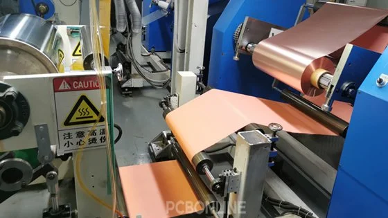
In this step, we also trim the edges and corners of the PCB laminates in case of burrs that affect PCB manufacturability.
Note: For ceramic PCB manufacturing, the start of PCB fabrication is to add the ceramic powder to the organic binder to make them paste ceramic slurry, and use a scraper to slice into pieces for further PCB production.
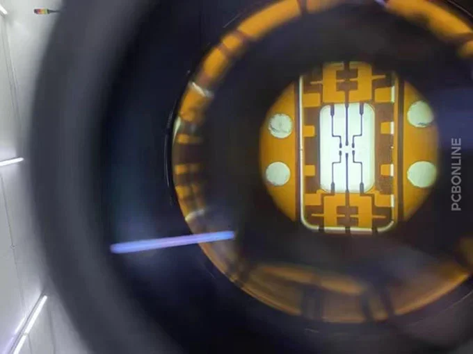
PCB fabrication step 2. Generating inner layer circuits
PCB fabrication of all types of PCBs has this step. The principle of generating inner layer circuits is graphic transfer by exposure and development.
First, we remove the contaminants on the PCB laminate surface and increase the roughness, which we call "pretreatment".
Then we paste a dry film on the copper surface of the PCB laminate by thermal forming. The dry film is a photosensitive plate film that reacts to cure under the light.
Then we put a PCB film above the photosensitive plate under UV light.
Note: The PCB film for the inner layer circuit is a negative film. It means in the copper foil, areas under the transparent areas of the PCB film are the wanted conductors and those under the black areas are removed during etching. For outer layer circuits, the PCB film, on the contrary, is positive.
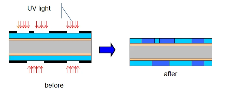
When the UV light shines on the photosensitive dry film through the transparent areas of the PCB film, there's a chemical reaction, and the photosensitive film cures. We call this process "exposure".
After that, we use the Na₂CO₃ solution to wash away the dry film that has no polymerization reaction. We call this process "development".
In this way, in the copper foil, the non-wanted areas are exposed, while the areas in the circuit graphic are covered by a cured coating.
Now we use an etching solution to etch away the exposed copper. This process is etching.
Then we a strong alkali NaOH to peel off the cured coating so that the inner layer circuit is exposed.
Now the inner circuit is generated! But wait, the inner layer circuit generation step does not end.
Keep in mind that an AOI (automatic optical inspection) is conducted when a circuit layer is generated.
At the end of inner layer circuit generation, we use an AOI machine to ensure the inner layer circuits are okay.
For multilayer PCBs with a copper layer quantity of 4 and above, the PCB inner layer quantity is 2 and above. All the inner layers' circuits are generated by the above method.
PCB fabrication step 3. Lamination
In this step, the inner copper layers and PP (prepreg) are stacked up alternately and laminated. PCB fabrication of all PCBs has the lamination step. It includes 5 processes, including roughening the copper surface, riveting, stacking layers, laminating, and post-processing.
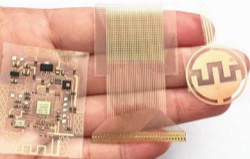
Note: PP, composed of resin and glass fiber cloth, is the insulating material used in FR4 PCB, ceramic PCB, and metal core PCB. For flexible PCB, the insulating material can be PI (polyimide) or PET (polyester). For high-frequency PCBs, the insulating material is PTFE.
At first, we roughen the inner layers' copper surface. We call this process "browning". By browning, the contact areas and wettability between the copper surface and PP are increased.
In the riveting process, we alternately stack up the inner copper layers and PP to be pre-stacked layers and nail them with rivets.
Note: If it is a 4-layer PCB, there's no riveting in the PCB fabrication process.
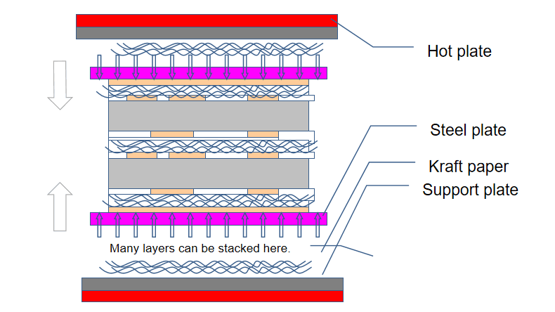
Next is the lamination process. We use kraft paper and steel plates to sandwich the pre-stacked layers and press them into a multilayer PCB at under high temperatures and pressure.
In the post process, we drill positioning holes and profile the entire board into a PNL (panelization) board.
PCB fabrication step 4. Drilling
For PCBs that have plating through holes (PTH), drilling is a necessary step in PCB fabrication. For FR4 PCB, high-frequency PCB, and metal core PCB, the PTH drilling method is mechanical drilling. For flexible PCB (including rigid-flex PCB) and ceramic PCB, the PTH drilling is laser drilling.
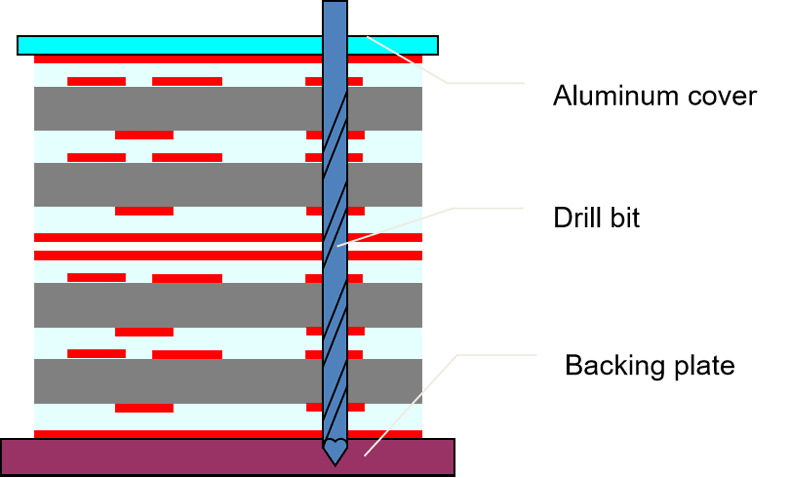
Note: In the high-frequency PCB manufacturing process, after drilling, we use the Plasma method to remove the drill dirt and any other contaminants in the hole walls. For HDI PCB manufacturing, the blind vias, buried vias, skipped vias, and stacked vias, the laser drilling is drilling each layer with micro vias separately.
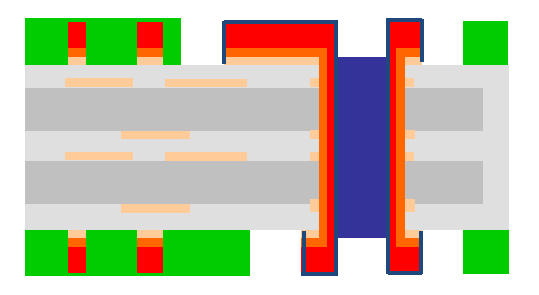
PCB fabrication step 5. Plating copper
Remember that the PTHs serve to conduct between different PCB layers, so the holes need to be plated with copper. To do this, first, we need to metalize the non-conductive PTH walls.
In the PCB fabrication process, this step includes electroless plating copper and electroplating copper.
In the electroless plating copper process, we use an activator to treat the resin and fiberglass cloth in the PTH walls to absorb a layer of palladium particles, which are active.
The copper ions are first reduced by the active palladium particles, and these reduced metal copper crystal nuclei become the catalytic layer of copper ions, allowing the reduction reaction of copper to continue on the surface of these new copper crystal nuclei.
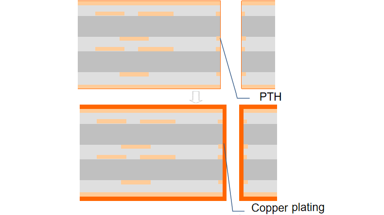
After the electroless plating copper process, there's a thin copper layer with a thickness of 0.5μm to 1μm. To protect the copper layer in the PTH wall, we electrically plate the PTH copper to increase its thickness from 5μm to 10μm.
The following step 6, step 7, and step 8 aim to generate the outer layer circuits so that all the PCB copper layers are interconnected and achieve electrical functions.
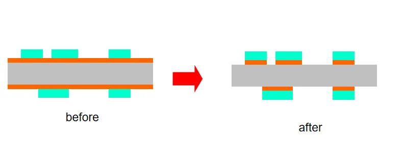
PCB fabrication step 6. Outer layer circuits
The process is similar to the inner layer circuits process, but here the PCB film is a positive one.
In the PCB outer layer circuit exposure process, the UV light makes the dry film on the non-wanted copper cure.
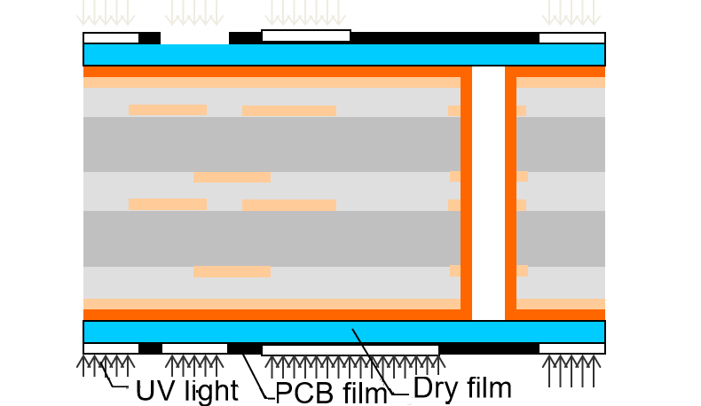
In the development process, the dry film on the circuit-graphic copper is washed away. After the exposure and development, the copper in the circuit graphics is exposed, and the non-wanted copper areas are covered by a cured coating.
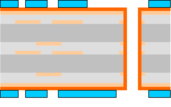
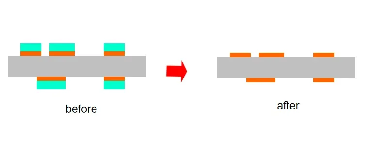
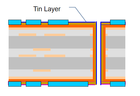
PCB fabrication step 7. Outer layer circuit plating
Now we electrically plate the copper in the circuit graphic directly. As this is the second time for copper plating, we call the process "secondary copper plating". We plate the outer layer circuits to be what copper thickness in the PCB design is.
Then we plate a tin layer on the outer layer circuit copper. Why do we do this? Because the non-wanted copper still exists and needs etching away, this tin layer will act as an etching resistor to protect the circuit graphic copper.
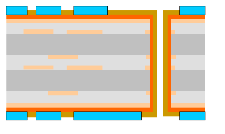
PCB fabrication step 8. Etching
Now the PCB fabrication process seems much clearer. Isn't it?
We peel off the cured coating using a chemical solution and etch away the unwanted copper.
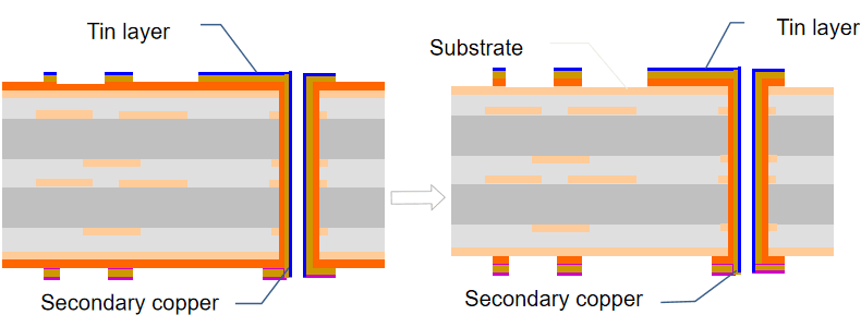
Then we peel off the tin layer on the outer layer circuit copper with another chemical solution.
So far, the basic of a PCB is fabricated. The next step is spraying a coating to protect the PCB copper circuits from damage.
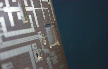
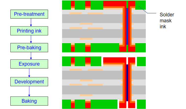
PCB fabrication step 9. Spraying solder mask
The solder mask is the protective coating of the PCB. It is made from silkscreen printing or spraying solder mask inks on the PCB and making to cure them.
Note: Not all PCBs have the solder mask. Naked PCBs that are used for verifying the design and debugging circuits have no solder masks so that the PCB designers can cut or connect the circuit traces on the PCB. For flexible PCBs, the protective coating is not a solder mask but a coverlay, which is a PI or PET film.
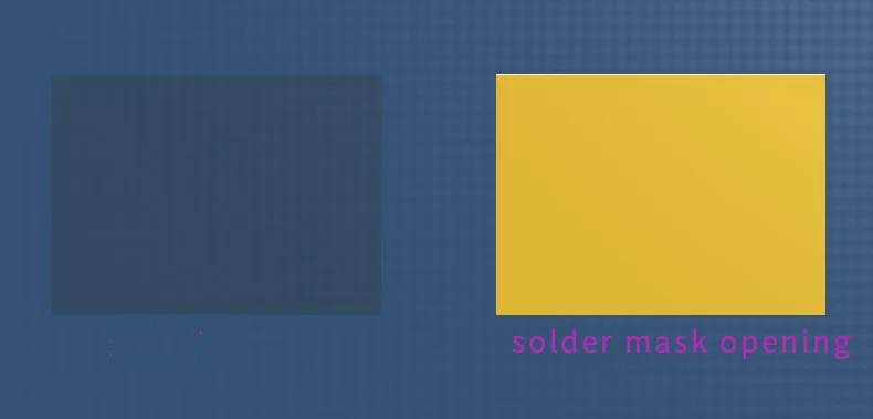
In a Gerber, there's a layer named "Top Overlay" or "Top Layer". That is the solder mask layer.
We silkscreen print or spray the solder masks on the PCB with strict adherence to this file.
For fabrication of FR4 PCB, metal core PCB, ceramic PCB, and high-frequency PCB, silkscreen printing and spraying solder mask are both okay.
For thick-copper PCB (>3oz) fabrication, we electrostatic spray solder masks on the PCBs.
PCB fabrication step 10. Spraying legend
On a PCB, you see the component codes, symbols, certification marks, company logos, etc. These are called legends or silk screens.
The legends are silkscreen printed on the solder masks and baked to cure.
PCB fabrication step 10. Surface finish
On a PCB, there are copper contacts that are expected to solder electronic components in PCB assembly. We call the contacts "PCB pads".
In the PCB fabrication process, it is necessary to spray a protective layer on the PCB pads to prevent them from oxidation or scratches. We call the protective layer on the copper contacts "surface finish".
The types of PCB surface finishes include OSP, HASL, immersion gold (ENIG), immersion silver, silver plating, carbon ink, hard gold plating, and ENEPIG.
The surface finish should be suitable for the type of PCB you design. Otherwise, the wrong surface finish can cause failures in PCB assembly or product use.
According to our 24-year PCB fabrication experience, immersion gold is a versatile surface finish. If you do not know which surface finish to use, you can choose immersion gold.
PCB fabrication step 10. Profile
On a PNL board, the PCBs are grouped. Whether it is PNL or a single PCB, we need to profile the board to create edges of the PCB so that it can be de-panelized for use.
For most PCBs, V-cut or punch is the most common way to profile PCBs. We punch the edges of FR4 PCB, MCPCB, and high-frequency PCB production panels to create grooves in about 2/3 deepness in a v-shape from the cross-section.
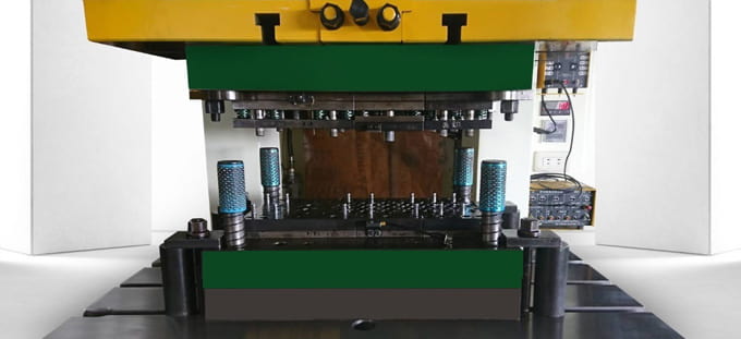
Besides, half-holes are also okay for FR4 PCB profiling.
However, to depanelize round ceramic PCB and flexible PCB (including rigid-flex PCB), we use the laser to cut the edges.
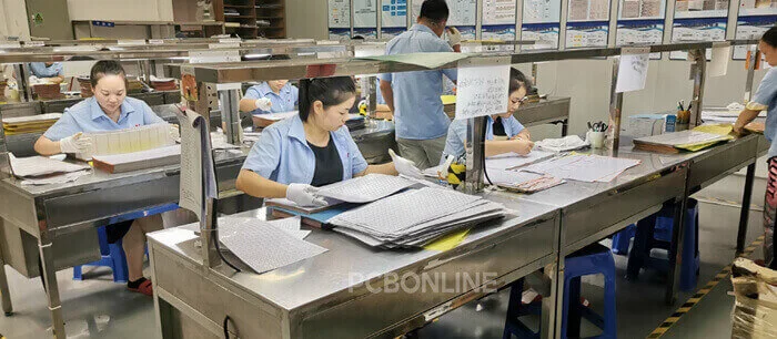
PCB fabrication step 10. Testing
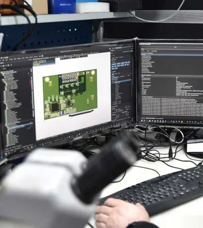
After the above PCB fabrication processes, the PCB is fabricated. Since we have had an AOI to each circuit layer, why do we still bother to test the boards? Because we haven't inspected the circuits of the entire PCB yet, and we can't ensure the PCB quality without the jig test and flying probe test.
A jig is also called a test fixture. It is a custom-made tool to test the electrical performance continuity of the PCB.
Besides, there is a flying probe test to test for opens and shorts in the circuits.
PCBONLINE, as an advanced PCB manufacturer, has an additional four-terminal sensing test (Kelvin test) to inspect the micro resistances of the PCBs. For automotive, defense, medical, and aerospace electronic products, this is a necessary PCB test to ensure the high performance of the product.
Is these PCB tests the end of the PCB fabrication process? Please keep patient, to ensure the PCB quality, there's still the final quality test below.
PCB fabrication step 10. Final quality tests
In the final quality tests, the PCB manufacturer strictly inspects the PCBs from the following aspects.
Dimension: The PCB manufacturer checks the outline dimension, hole to edge, PCB thickness, hole diameter, trace width/space, annular rings, bow/twist, and PCB via plating thickness.
Surface: The PCB manufacturer checks whether there's any void, hole plug, copper exposure, foreign particle, extra/missing hole, gold finger defect, or legend defect in the PCB.
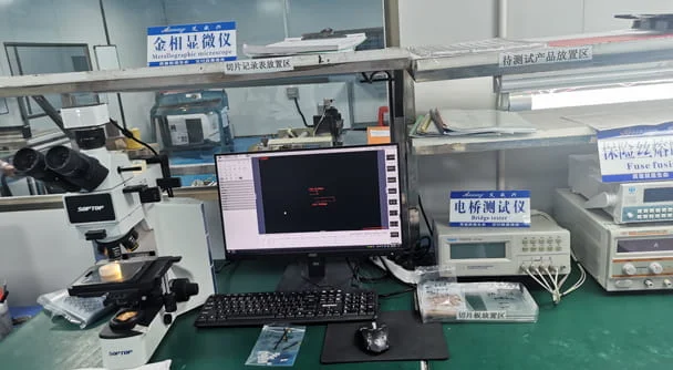
Reliability: The PCB manufacturer has various tests to ensure the PCB solderability, peel strength, micro strength, S/M adhesion, gold adhesion, thermal shock, impedance, and ionic contamination.
Note: For high-frequency PCB fabrication, the thermal shock test is necessary. It is 1 to 3 times depending on the PCB requirements, and each time the thermal shock at 288℃ lasts 10 seconds.
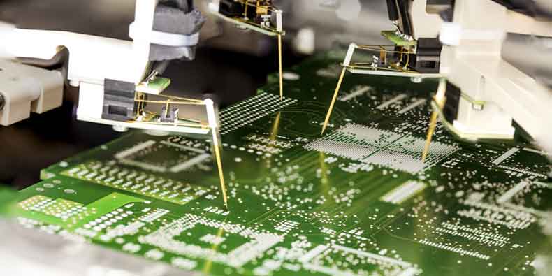
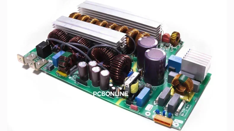
PCB Assembly
The PCB assembly process includes SMT manufacturing and through-hole assembly. You can check out their detailed process from the previous blogs.
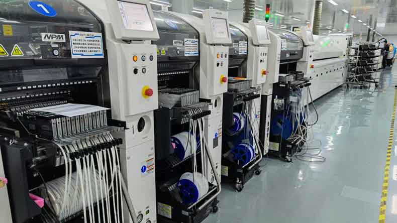
The SMT manufacturing process is roughly divided into these steps: solder paste printing, solder paste inspection, placing components, X-ray inspection, reflow soldering, and AOI.
After the SMT assembly, if there are PTH holes in the PCB, here is the PTH assembly with these steps: inserting component leads through PTH holes > wave soldering > trimming the leads and visual check.
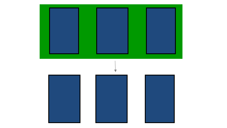
After PCB fabrication and assembly, the PCB manufacturer can depanelize the single PCBAs from the PNL without any harm using the automatic depanel machine.
In the post-assembly process, the EMS PCBA manufacturer PCBONLINE can provide value-added services, such as functional testing, IC programming, conformal coating, thermal aging, and box-build assembly.
After the end products pass the application simulation test, it is the end of all PCB fabrication and assembly processes.
PCB fabrication, PCB assembly, and box-build assembly are flexible production. You tell your contract manufacturer (CM) what you need, and your CM provides electronic manufacturing services for you.
Plus, as electronic contract manufacturers start having their R&D capability, you can have PCB fabrication and assembly without designing the PCB by yourself. There are ODM (original design manufacturer) and EMS (electronic manufacturing service) manufacturers that both provide design and PCB fabrication and assembly.
If you want to work with a CM for PCB fabrication and assembly, you can contact PCBONLINE by email at info@pcbonline.com. PCBONLINE has strong manufacturing capabilities to independently finish the PCB fabrication and assembly process for any type of PCB. Besides, it has its R&D team, which provides on-the-shelf ODM solutions and PCB/product design. You can have PCB fabrication and assembly at PCBONLINE from prototypes to bulk production at one stop.
Conclusion
This article is perhaps the most original and comprehensive guide to the PCB fabrication process on the internet so far. It reveals the PCB fabrication process of not only FR4 PCB and metal core PCB, but also the advanced PCBs such as ceramic PCB, high-frequency PCB, flexible PCB, and HDI PCB. Besides, this article illustrates the PCB fabrication process step by step, and each step gives details of the process. If you need PCBs or PCBA and still have doubts about your design or project, talk with PCBONLINE to solve them now.
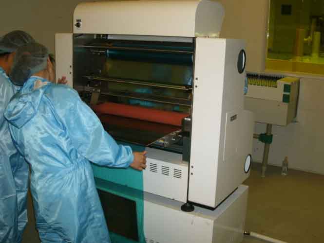
PCB fabrication at PCBONLINE.pdf