Advantages of the PCB Fabricator PCBONLINE
 MATERIALS
 At PCBONLINE, you can have advanced PCBs made of any substrate material, such as FR4, PTFE, aluminum, ceramics, copper, polyimide, polyester, and glass.
 EQUIPMENT
 PCBONLINE has two large advanced PCB manufacturing bases and one PCB assembly factory, with complete PCB fabrication lines, and can independently finish all types of PCB fabrication.
 TEAM
TEAM The professionals from PCBONLINE offer free PCB DFM and one-on-one engineering support throughout your project, and they can take part in the R&D if you want.
 PCB QUALITY
 The advanced PCBs at PCBONLINE are military, automotive, and medical-grade. The PCB fabrication is certified with ISO, IATF, REACH, RoHS, UL, and IPC standards.
 CUSTOM
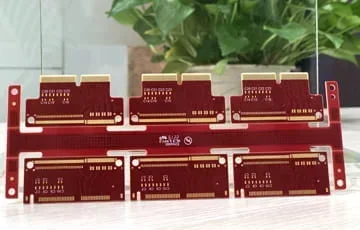
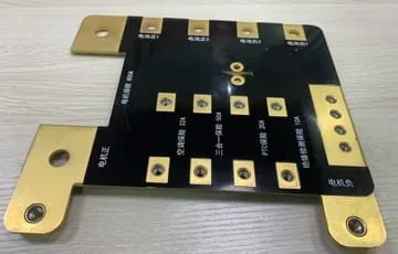
 PCBONLINE provides all types of PCB fabrication, including FR4 PCB, MCPCB, ceramic PCB, RF PCB, HDI PCB, flex PCB, and rigid-flex PCB, with no quantity limit.
 TRANSPORT
 PCBONLINE provides PCB shipping methods, including air, sea, and rail shipping by DHL, FedEx, and UPS. You can choose your freight forwarder.
Types of PCB Fabrication and Capabilities
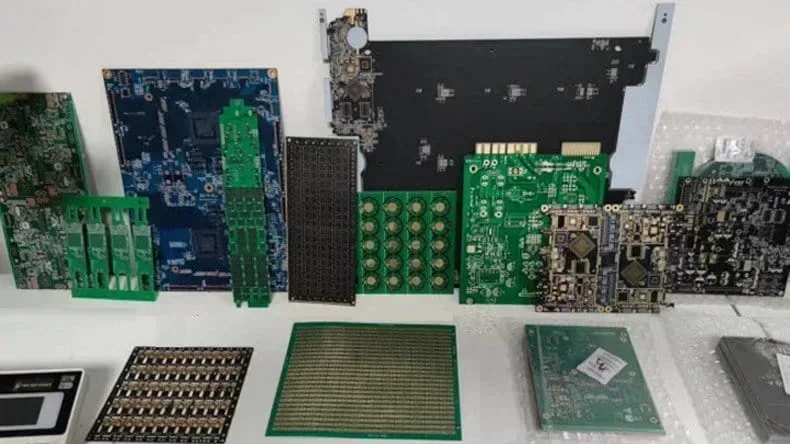
PCB is a printed circuit board, also called a PWB, printed wiring board, or circuit card. The fabrication of PCBs varies for different types of PCBs. At the one-stop PCB fabricator PCBONLINE, PCB fabrication includes rigid PCBs, flexible PCBs, rigid-flex PCBs, ATE (Automatic test equipment) boards, and hybrid-structure boards. Please check the capabilities of different types of PCB fabrication.
Rigid PCB fabrication includes FR4 PCB, metal-core PCB, ceramic PCB, HDI PCB, high-frequency PCB, and special material rigid PCB.
PCB fabrication layer count: 1-80L (aluminum and ceramic PCB 1 to 4, copper-core PCB 1 to 8)Maximum PCB fabrication thickness: 10mmMinimum PCB fabrication thickness: 0.12mm (2L), 0.18mm (4L)PCB fabrication thickness tolerance: thickness≤1mm: ±0.1mm, thickness>1mm: ±10%Maximum PCB fabrication size: 1100mm * 570mm (metal-core PCB 1200mm * 500mm)Minimum PCB fabrication size: 10mm * 10mmSpecial product/material: use adhesive or PP to laminate stiffener on the rigid PCB, rigid PCB need overlay to replace soldermask, step embedded conductor/slot, embedded resistance, embedded capacitance, embedded component, PET material, black FR4 (e.g. VT42B...), Polymide material for rigid PCB (e.g. 85N/VT-901), hole wall thickness >=50um, and JQ aluminum PCBHybrid-structure PCB with UL: RO4350B+S1170, RO4350B+IT180A, TU-752/TU-768F/TU768/TU788+M6
Flexible PCB fabrication capabilities:
Layer count: 1-8L (1-4L normal)Board thickness: 0.1mm-0.5mm (1-4L), 0.6mm-0.8mm (5-8L)Maximum finished board size: 7.8inch * 21.8inch (PI≥1mil), 7.8inch * 14inch (normal)Minimum finished board size: 2mm*4mm (no connection tab), 8mm*8mm (with connection tab)Flex PCB fabrication materials: adhesive flex core, adhesiveless core, coverlay, thermosetting adhesive, PI/FR4/steel stiffener, and 3M tapeOutline tolerance of laser cutting: ±0.05mm
Rigid-flex PCB fabrication capabilities:
PCB layer count: 2-24LFlex layer count: 11-20L (18L)Flex layer on outer layer or middle layer: MiddlePCB Board thickness: 0.2mm-4.0mmTolerance of PCB board thickness: >1.0mm, ±10%; ≤1.0mm, ±0.1mmMinimum flex width: 2.5mmMinimum flex width between rigid: 3mm, 2mm(limit)Maximum PCB panel size: 406mm * 736mmMinimum PCB panel size: 10mm * 15mm
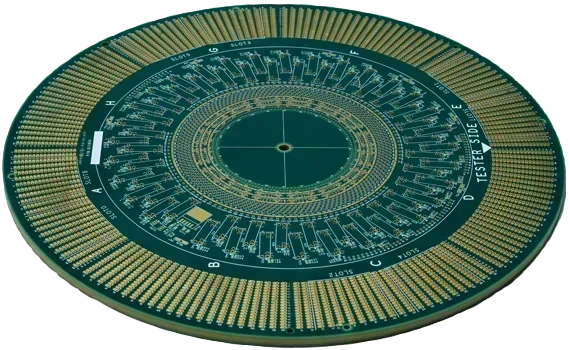
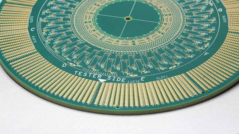
ATE board fabrication includes load Board, probe card, interposer, interface board, and BIB (burn-in board).
PCB thickness tolerance: ≤7% (level 1), 5% ≤ level 2 < 7%Maximum board size: 50mm*50mm≤level≤1570mm*660mm, 610mm*710mm (level 2)PCB layer count: ≤50 (level 1), >50 (level 2)PCB thickness: 0.4mm≤level 1≤8mm, 8
Please get in touch with our sales staff for a detailed process capability table, and we will send it to you via email for your reference. You can send emails to info@pcbonline.com or chat with us online.
Technologies and PCB Fabrication Prices
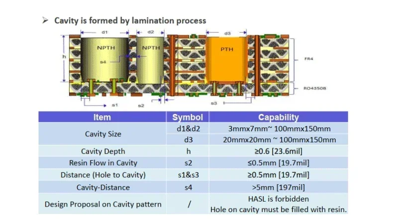
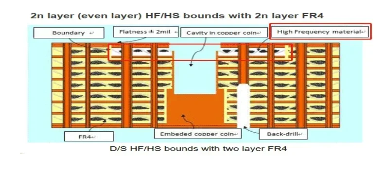
PCBONLINE is a one-stop PCB manufacturer that provides on-demand PCB fabrication to meet the needs of different companies, institutes, and business makers. We offer advanced PCB fabrication technologies, including local mixed pressure, embedded copper coin, and cavity technologies.
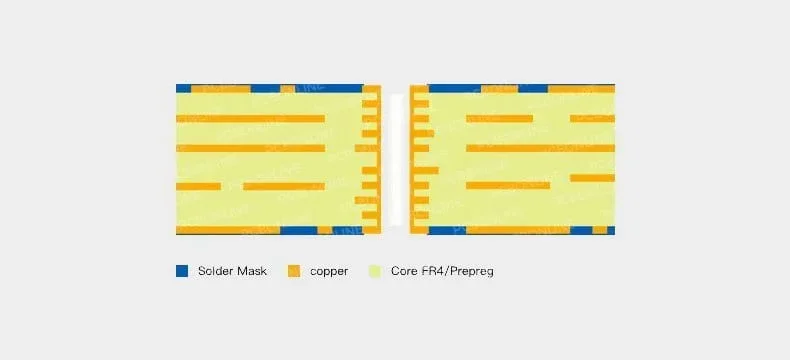
Partially hybrid structure lamination: Different laminate materials are laminated in the same layers at different areas or in different layers for certain purposes, such as better thermal dissipation, smaller electromagnetic interference, etc.Embedded copper coin: Also known as thermoelectric separation technology for copper base PCB. By embedding the copper coin to connect the copper base and the PCB contact directly, the thermal generated by the working component, such as an IC, is dissipated at once without overheating concern.Cavity: The cavity is formed by the lamination process. The depth of the NPTH and PTH is controlled.
The price of PCB fabrication depends on the PCB board's complexity, fabrication processes, materials, and quantity.
Generally, more PCB layers and higher copper thickness lead to a higher PCB fabrication cost. Simple PCBs are cheaper than advanced PCBs. The unit price of bulk production is lower than PCB prototypes. The ceramic PCB prototype price is calculated by PCB piece. Prices of flexible and rigid-flex PCBs are calculated according to their weight.
Here are some PCB fabrication prices for your reference: At PCBONLINE, $200 is enough to have the dual-sided flexible PCB prototypes manufactured with PCBA value-added services included. If you order 4-layer PCB with a total area of 0.1 square meters, for example, it costs about $100 for FR4 PCBs, $400 for flexible PCBs, and $1000 for rigid-flex PCBs.
As a source factory PCB fabricator, advanced PCB fabrication at PCBONLINE is probably one of the most affordable. If you order PCB assembly services or PCBA ODM manufacturing, you will find more surprises from PCBONLINE in meeting your custom demamds.
PCB Fabricator PCBONLINE
Founded in 2005, the PCB fabricator PCBONLINE has two large advanced PCB manufacturing bases, one PCB assembly factory, and an R&D team to offer ODM solutions. We are a group of professional technology-originated teams, including 100+ software and hardware engineers and 500+ technicians, providing you with complete PCB fabrication services, such as project optimization, choosing materials, testing methods, Gerber and BOM checkout, quality verification, component sourcing, PCB assembly, and box-build assembly.
PCBONLINE provides not only PCB fabrication but all services related to your PCB project, including R&D, DFM, design for testing (DFT), prototyping, and solutions to technical issues.
If you need PCB assembly, PCBONLINE also provides PCB design for assembly (DFA), PCBA, and post-assembly services such as box builds.
For PCB fabrication, please send your Gerber to info@pcbonline.com. The professionals at PCBONLINE will review your Gerber and give a quick reply.
Printed Circuit Board Fabrication Capabilities
Applications of PCB fabrication:
military and aerospace electronics. Successful examples include military Rogers PCBs and aircraft PCBmiddle and high-end consumer electronics. Successful examples include UV disinfection boxes and earphonescomputing and communication electronics. Successful examples include web server fabricationautomotive and medical electronics. Successful examples include gastroscopy and flexible clear PCBs for car
GET A FREE QUOTE
PCB and PCBA Certifications


Contact Our Expert Team Now

Learn about our products


Get customized services

 Phone
Phone WhatsApp
 Email
Email
Offer Electronics Manufacturing All-in-One
PCBONLINE® is a registered trademark or service mark of pcb online limited or its affiliates.
Copyright © 2005-2025 Pcb Online Limited. All rights reserved


