Advantages of the PCB Manufacturer PCBONLINE
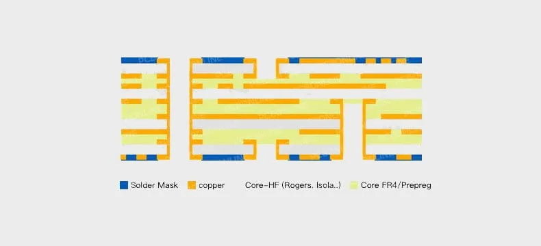
 MATERIALS
 In-stock high-frequency PCB materials of low Dk, Df, thermal expansion coefficient, and water absorption for PCB fabrication from PCBONLINE.
 EQUIPMENT
 PCBONLINE has specialized Plasma treatment equipment for the electroless copper deposition step in the high-frequency PCB fabrication process.
 TEAM
TEAM The professionals from PCBONLINE grasp the core technology to minimize the expansion and contraction of the RF microwave PCBs.
 QUALITY
 High-frequency PCB materials storage time at PCBONLINE remains no more than 45 days to make sure the PCB quality.
 CUSTOM
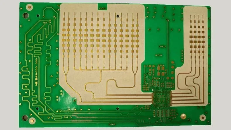
 We can realize embedded conductor design structures and low-sensitivity antenna layers and make RF interface and digital interface on the same high-frequency PCB.
 TRANSPORT
 PCBONLINE provides various high-frequency PCB shipping methods, including air, sea, and rail shipping by DHL, FedEx, and UPS. You can choose your freight forwarder.
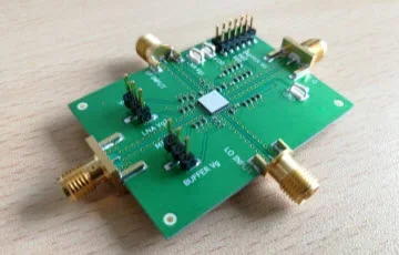
3 Types of High-Frequency PCBs
High-frequency high-speed PCBs transmit and receive 50MHz to 100GHz high-speed/microwave/radio frequency signals. Here are 3 types of high-freuqnecy PCBs:
● High-requency PCBs from 6GHz to 24GHz: RF 6GHz to 24GHz PCBs are used for signal emission and reception within 30 meters.
The RF circuit generates a radar lobe, and the PCB antenna structure emits it. The radar lobe is reflected by the object and received by the antenna structure.
To optimize circuit functions, PCBONLINE uses materials of higher frequencies and manufactures the PCBs to have a stable and small dielectric constant and dielectric loss.
● High-requency PCBs 77GHz: RF 77GHz PCBs are used for signal emission and reception at a longer distance and provide a higher resolution.
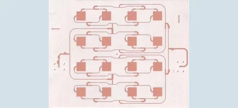
In a radar PCB, two antennas are integrated into the circuit board as the etched copper structure. One antenna is the radar wave transmitter, and the other is the radar wave receiver.
The high-frequency circuit generates the waves and evaluates the reflected signal. Usually, the RF part on the front side of the high-frequency PCB emits the wave, and the digital circuit on the backside evaluates the reflected signals.
PCBONLINE manufactures RF 77GHz PCBs to have a much smaller antenna structure, conductor geometry, and manufacturing tolerances.
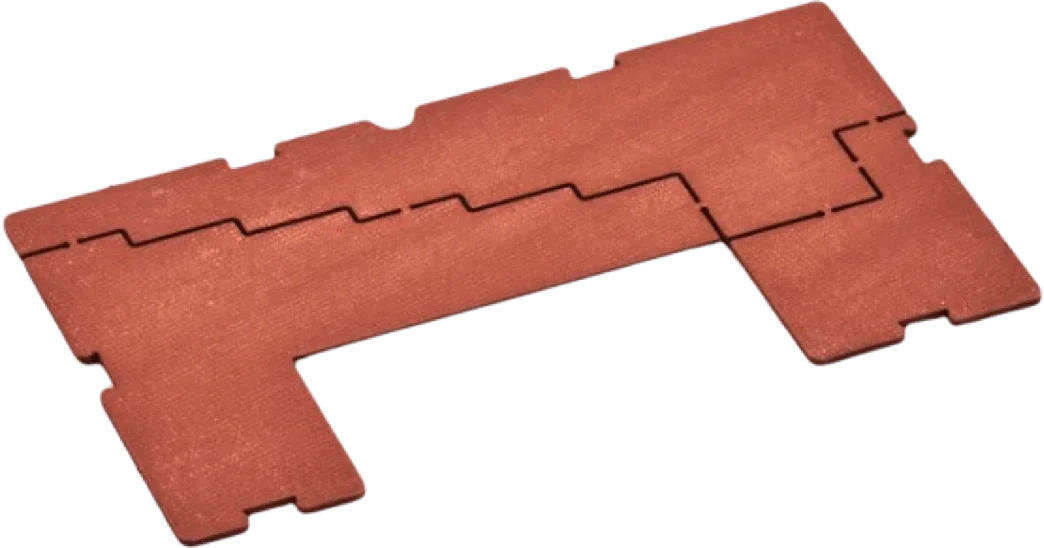
● Embedded Antenna PCBs: Embedded antenna PCBs are developed from RF 77GHz PCBs.
The conductive pattern in the PCB RF layers is embedded in the RF material so that the PCB can be manufactured to have a small conductor space/width, minimized conductor tolerance, and rounded corners.
Besides, accurate mapping of the antenna layout improves the RF performance and reduces power consumption of the RF microwave PCB.
PCBONLINE's embedded antenna DFM can minimize the PCB's conductor tolerance and corner roundness/roughness.
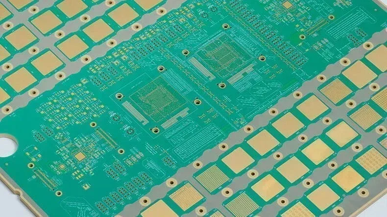
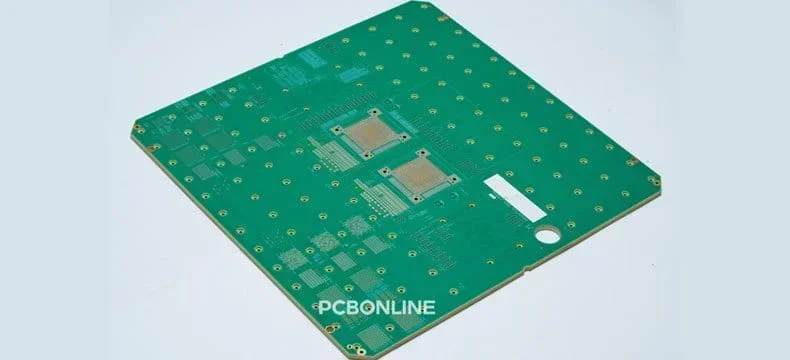
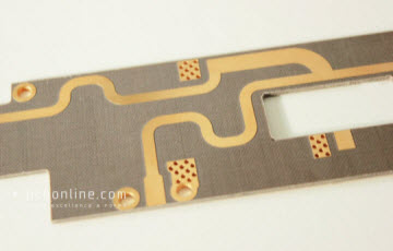
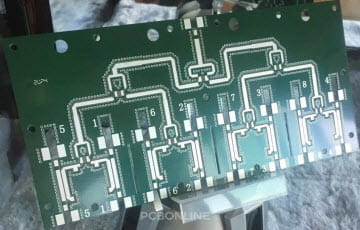
High-Frequency PCB Manufacturing at PCBONLINE
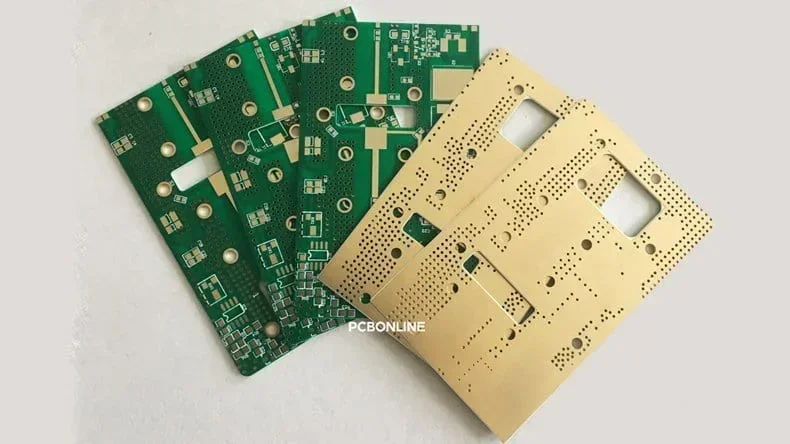
PCBONLINE provides one-stop high-frequency PCB manufacturing, from choosing PCB materials, prototyping, to batch PCB assembly and testing.
Here are some key points in high-frequency PCB manufacturing from PCBONLINE.
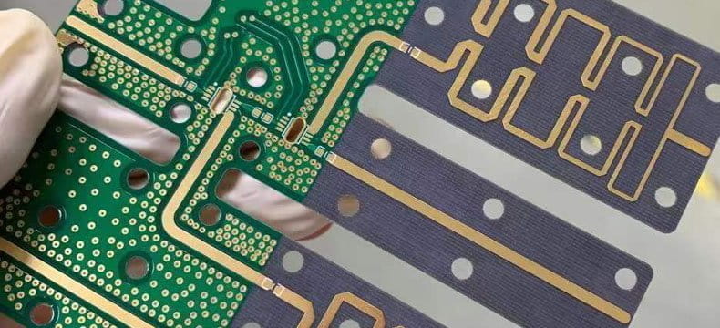
Our engineers compensate the trace width according to different copper thicknesses and measure the etched copper thickness to confirm it is within the tolerance range of ±0.02mm (but can even be ±0.015mm).After the film is drawn, we check and make sure no pinholes or gaps in the film. Pit, notches, pinholes, and other defects in the circuit lines will affect the transmission effect, and we allow no such minor defects in the high-frequency PCBs.We adopt the Plasma method for chemical copper sinking, which is the most difficult procedure of high-frequency PCB fabrication. All holes must have copper and we allow no blank. We inject carbon tetrafluoride (CF₄) or argon (Ar₂) nitrogen (N₂) and oxygen (O₂) between two high-pressure electrodes under the vacuum environment, and we place the high-frequency PCB between two electrodes. In this way, the Plasma is formed in the cavity to remove the drilling dirt and dirt in the hole.Solder resistance thickness is also strictly controlled. Because too thick or too thin lines solder masks for several microns can be disqualified.The final destructive test is carried out in manufacturing: thermal shock at 288℃ for 10 seconds, for 1 to 3 times, to ensure no separation of hole wall.
Besides, engineers from PCBONLINE have comprehensive coordination with the client throughout the high-frequency high-speed PCB project. With a correct understanding of the client's needs and product functionality, PCBONLINE providea useful improvement suggestions and manufacture high-frequency PCBs yielding satisfying results.
Advantages of High-Frequency High-Speed PCBs
High-frequency PCBs usually adopt the PTFE or ceramic high-frequency materials for the substrate and thus have these advantages:
Have a small and stable dielectric constant (Dk), which prevents signal transmission delay.Have a small and stable dielectric loss (Df), which reduces RF microwave signal losses.Have a low and consistent thermal expansion coefficient (CTE), which prevents copper foil separation.Have a good impact strength, peel strength. and thermal/chemical resistance.
With good materials and expertise, PCBONLINE manufactures high-frequency PCBs to have a small impedance tolerance and optimized RF performance. You can contact info@pcbonline.com to get a quote.
High-Frequency PCB Manufacturing Capabilities
Applications of High-Frequency PCBs
Communications facilities, such as signal towers, antennasSatellite communications systemsAircraft and automotive collision avoidance systemsFilters, couplers, power amplifiersRF microwave devices, such as backhauls, sensors, adaptersConsumer electronics, such as smartphones, GPS
GET A FREE QUOTE
PCB and PCBA Certifications


Contact Our Expert Team Now

Learn about our products


Get customized services

 Phone
Phone WhatsApp
 Email
Email
Offer Electronics Manufacturing All-in-One
PCBONLINE® is a registered trademark or service mark of pcb online limited or its affiliates.
Copyright © 2005-2025 Pcb Online Limited. All rights reserved


