Advantages of the PCB Manufacturer PCBONLINE
 MATERIALS
 PCBONLINE uses materials of low dielectric loss for HDI PCB, such as Isola I-speed and Isola Tachyon 100G. We can help you choose HDI PCB materials.
 EQUIPMENT
 PCBONLINE has 4 manufacturing bases equipped with specialized equipment for HDI PCB manufacturing. 3000m² of HDI PCB capacity per day.
 TEAM
TEAM 1000 employees at PCBONLINE provide an extensive range of technologies and end-to-end HDI PCB solutions, from the initial idea to high-volume production.
 QUALITY
 PCBONLINE's precise and controllable mechanical deep drilling expertise empowers HDI PCB technological possibilities and ensures the best PCB quality.
 CUSTOM
 PCBONLINE provides custom HDI PCB design and manufacturing, with varying copper thicknesses in HDI PCB manufacturing.
 TRANSPORT
 PCBONLINE provides various HDI PCB shipping methods, including air, sea, and rail shipping by DHL, FedEx, and UPS.
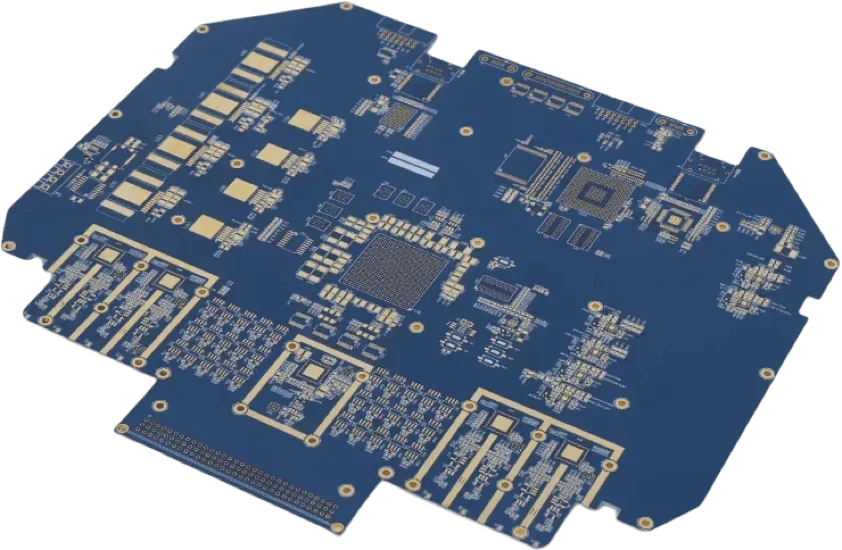
HDI PCB vs Microvia PCB
HDI PCB is a high-density-interconnected printed circuit board. High-density PCB is slao known as microvia PCB.
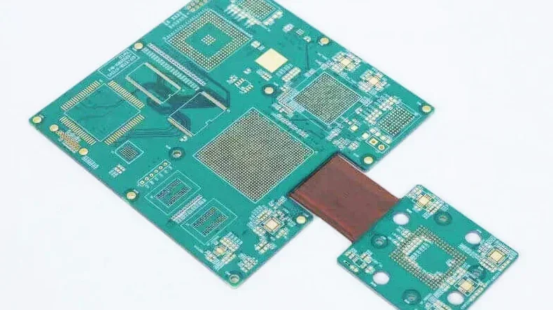
Many PCB design can be high-density, including flexible PCB, FR4 PCB, and rigid-flex PCB.
On the two sides of an HDI PCB, the number of electrical connections on average is 20/cm² or 130/in². And the trace width and space are equal to or smaller than 100µm or 0.004''.
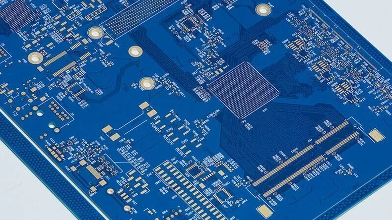
A microvia is laser drilled. It has an aperture equal to or smaller than 0.15mm or 0.006'' and penetrates only one PCB layer.
An HDI PCB typically has microvias in SMT pads. For this reason, microvia PCB is another name for HDI PCB.
Besides, the microvias of an HDI PCB can stack to form blind or buried vias.
A blind hole penetrates from the external layer to an external layer, while a buried hole penetrates from an external layer to another.
In HDI PCBs, microvias can be single, staggered, stacked, or skipped. The smaller the microvia aperture, the smaller the parasitic capacitance, which is practical for high-speed circuits.
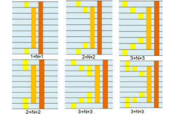
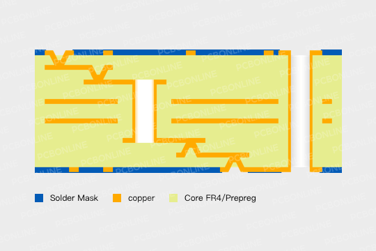
HDI PCB Stackup and Lamination
HDI PCB manufacturing requires sequential lamination. For example, 3+N+3 means the HDI PCB requires three times laser drilling and laminations.
In a HDI PCB stackup, the number of microvia pairs stands for how many times of lamination in HDI PCB manufacturing.
At the HDI PCB manufacturer PCBONLINE, the HDI PCB fabrication has a maximum lamination cycle of 8.
Duaring HDI PCB lamination, the internal layers without microvias are laminated in the standard lamination way under high temperatures and high pressure.
Prepreg melts, fills in gaps between adjacent copper layers and solidifies so that the copper layers are bonded and insulated.
Lamination to external layers with microvias of an HDI PCB is more difficult than internal layers.
Microvias are laser dilled before lamination, and after lamination, microvias on different layers may overlap to form stacked vias or stagger to form staggered vias.
Positioning for laser drilling and lamination should be highly accurate. Otherwise, the board defects. So HDI PCB manufacturing costs more than normal PCBs.
Advantages of HDI PCBs
HDI PCBs are suitable for products where electrical performance and noise rejection are of utmost importance.
The advantages of HDI PCBs include:
● HDI technology decreases products' overall size and improves electrical performance.
● HDI PCBs have great impedance control and impressive high-frequency transmission capabilities.
● HDI PCBs offer a perfect solution for fine pitch packages, flip-chip assemblies, and complicated BGA designs.
High-Density PCB Manufacturing Capabilities
Applications of high-density PCB:
battery switches and power distributorsmotor controls and LED applications controlautomotive, industrial, communications electronicssatellites, microsystems
GET A FREE QUOTE
PCB and PCBA Certifications


Contact Our Expert Team Now

Learn about our products


Get customized services

 Phone
Phone WhatsApp
 Email
Email
Offer Electronics Manufacturing All-in-One
PCBONLINE® is a registered trademark or service mark of pcb online limited or its affiliates.
Copyright © 2005-2025 Pcb Online Limited. All rights reserved


