
A flexible PCB, abbreviated for FPC, is a polyimide (PI) or polyester (PET) based printed circuit board that can bend and fold. Flexible PCBs can be single-sided, double-sided, yellow, black, white, and transparent. They are light, and thin, and are widely used for applications where flexibility is required.
![]()
How do FPC manufacturers fabricate flexible PCBs? The one-stop flexible PCB manufacturer PCBONLINE took an FPC factory video below.
Our factory not only fabricates flexible PCBs but also PCB laminates. For your reference, we illustrate the flexible PCB manufacturing process step by step.
- Step 1. Fabricating Flexible PCB Laminates
- Step 2. Cut Laminates for FPC Fabrication
- Step 3. Drilling
- Step 4. VCP Electroplating
- Step 5. Circuit Transfer (Exposure)
- Step 6. Etching
- Step 7. Drilling Positioning Holes
- Step 8. Electrical Test
- Step 9. Cleaning and Scrubbing
- Step 10. FPC Layers Alignment and Lamination
- Step 11. Printing Silkscreen
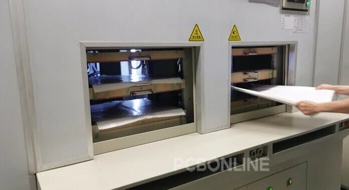
- Step 12. Baking Flexible PCBs
- Step 13. Surface Finish
- Step 14. Finished FPC Electrical Test
- Step 15. Forming Flexible PCBs
- Step 16. Visual Inspection
- Step 17. Sampling Testing
- Step 18. Packaging and Warehousing Before Delivery
Note: Except for visual inspection and packaging, all the other steps are completed on machines. The machines are set up with programs designed by our CAM (computing assistance manufacturing) engineers. Technicians operate the machines according to our factory's standard operating procedures.
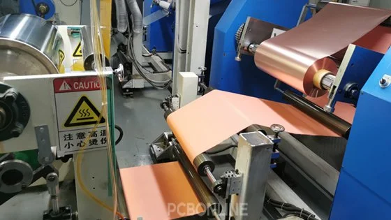
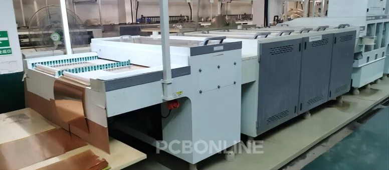
Step 1. Fabricating Flexible PCB Laminates
![]()
When confirming everything about your flexible PCB design and order, PCBONLINE orders the rolled copper or electrolytic copper foil, PI, and adhesive for flexible PCB laminates.
On the copper foil line, we press the copper foil to be in the required thickness. On the other line, we brush the PI film with adhesive and laminate them at high temperatures and pressures to form the coverlay, which plays the same function as the PCB solder mask.
![]()
From PCBONLINE, the available PI thicknesses can be 12.5μm, 25μm, 50μm, and 75μm. The copper thicknesse include 12μm, 18μm, 35μm, and 70μm. The adhesive thickness generally is 20μm.
Step 2. Laminate Coverlay and Copper Foil
The PI film coverlay is already brushed and laminated with adhesive before going on the FPC fabrication lines. So the first step is to laminate the coverlay and copper foil. In the next steps, we drill holes and generate circuits on the other side of the copper.
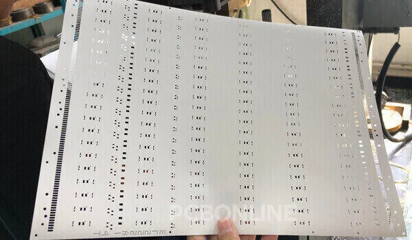
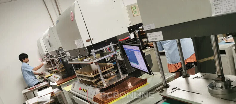
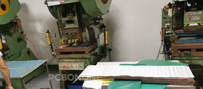
Step 3. Drilling
![]()
This step is laser drilling PTH holes on the FPC copper laminates. The PTH holes need copper electroplating. Different circuit layers of the flexible PCB are interconnected by PTH holes.
At PCBONLINE, the minimum PTH hole aperture is 0.2mm. The hole aperture tolerance is ±0.05mm. The finest pitch between adjacent PTH holes is 0.3mm.
Note: For openings on FPC coverlay, we can adopt the more economical mechanical drilling method (the opening is in the oval shape that may be different from your original design), and we can also adopt the punching method (the opening is square or rectangular and the same as your design).
Step 4. VCP Electroplating
In our flexible PCB factory, PTH holes are electroplated with copper on the VCP (vertical continuous plating) line. The VCP technology offers even PTH via wall copper thickness to flexible PCBs.
Step 5. Circuit Transfer (Exposure)
The copper laminate is printed with a UV-sensitive photoresist layer. A film with the circuit image is placed above the copper laminate under UV light. In this way, copper in the circuit image is protected by the cured photoresist, and the photoresist on the other copper areas is still liquid.
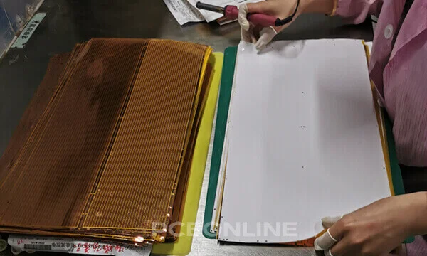
Step 6. Etching
The etching machine is very long, with many modules. In the etching process, the NaOH solution solves the other copper areas, and only copper in the circuit image remains due to the protection of the cured photoresist.
In the last modules of the etching machine, the cured photoresist is also washed away.
From PCBONLINE, the finest pitch between a pad to an adjacent trace is 0.35mm. The minimum trace width/space is 0.15mm/0.15mm. The trace width/space tolerance is 0.05mm.
Now, the whole copper layer has only the copper circuit traces and pads.
Step 7. Drilling Positioning Holes
Positioning holes are used to fix the flexible PCBs during the electrical tests and the forming of the finished FPCs. There are usually 3 positioning holes in the diagonal direction on the flexible PCBs.
Drilling positioning holes is mechanical drilling.
Step 8. Electrical Test
Whenever a circuit layer is etched out, it needs an electrical test. We place each flexible PCB on a jig to conduct the power-on self-test to ensure the circuit is okay.
Step 9. Cleaning and Scrubbing
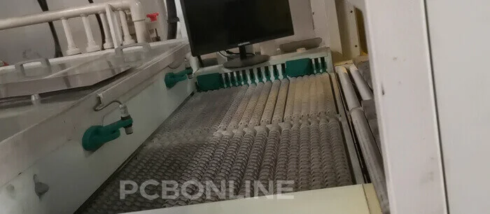
The cleaning and scrubbing line is an assistance line for flexible PCB fabrication. The flexible PCBs are sent into the cleaning and scrubbing machine to remove the oxide, residual NaOH, and moisture. The flexible PCBs are also scrubbed to increase the gloss.
Step 10. FPC Layers Alignment and Lamination
The PI and adhesive have already bonded with each other. What we need to do now is to align the copper layer with PI and adhesive so that they can be laminated.
After aligning the flexible PCB layers, we place them in a lamination machine that works at high temperatures.
Step 11. Printing Silkscreen
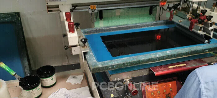
At this step, we place flexible PCBs in a silkscreen printing machine to print the marks, symbols, and logos on the flexible PCBs.
Step 12. Baking Flexible PCBs
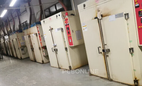
We bake the flexible PCBs so that the silkscreen gets dry.
Step 13. Surface Finish
After the solder mask and silkscreen are applied on flexible PCBs, we need to do the surface finish to the exposed copper pads.
At PCBONLINE, for immersion gold, the nickel thickness range falls from 0.2µm to 0.5µm, and the gold thickness range falls from 0.01µm to 0.05µm. For immersion tin, the thickness range falls from 0.4µm to 0.6µm. For the anti-oxidation film, the thickness range falls from 0.3µm to 0.45µm.
Step 14. Finished FPC Electrical Test
Now the flexible PCBs are laminated and printed with silkscreen. The FPC fabrication is done. Now we implement the electrical test again to ensure the flexible PCBs' circuit is okay.
Step 15. Flexible PCB Profile
Profiling flexible PCBs means cutting the edge rails to separate PCBs on a production panel.
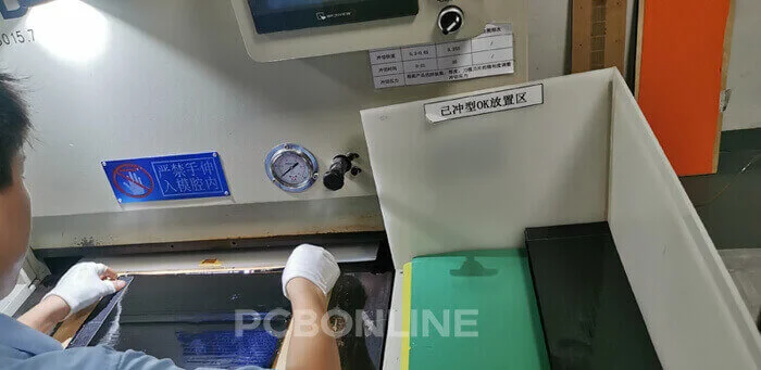
For the edges that are vertical/horizontal straight lines, we use cutting dies to cut the edge rails on the production panels.
For edge rails that are irregular, such as triangles, we use steel dies to cut the edge rials.
If the edge rails include both regular straight lines and irregular lines, we use cutting dies first and then steel dies.
At PCBONLINE, the cutting die forming tolerance is 0.2mm, and the steel die forming tolerance is 0.1mm.
Step 16. Visual Inspection
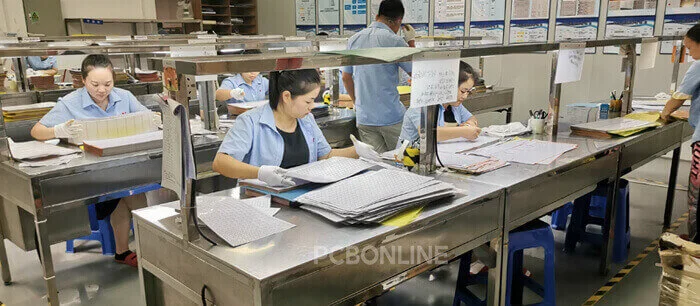
Our experienced technicians visually inspect the completed flexible PCBs to ensure no contamination or scratches. Meanwhile, they will also count the flexible PCB number to ensure the quantity is correct.
Step 17. Sampling Testing
Now all flexible PCB fabrication processes are completed. We randomly pick up some samples (6% to 10%) from the finished flexible PCBs to test the boards. This is part of our quality control.
If there are errors in the samples, we will test 100% of the flexible PCBs to ensure no defective FPCs delivered to our clients.
Step 18. Packaging and Warehousing Before Delivery
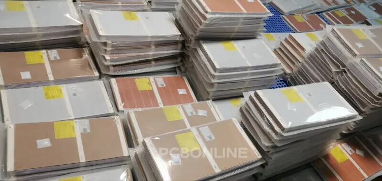
We will package the flexible PCBs according to your requirements and temporarily store them in our warehouse.
In regards to the flexible PCB delivery, we recommend FedEx for shipping, which has a cooperation with us, and it's cheap. You can also choose UPS and DHL.
Why PCBONLINE for One-Stop Flexible PCB Fabrication
The above shows how flexible PCBs are fabricated from PCBONLINE's FPC factory. Besides flexible PCB fabrication, PCBONLINE can also do flexible PCB assembly and source the electronic components. Founded in 1999, PCBONLINE has rich experience in flexible PCB design, fabrication, and assembly.
You can get FPC design, laminates, fabrication, and assembly under one roof from PCBONLINE to save time and costs.
We provide 1 to 8-layer flexible PCBs, including single-sided, double-sided, with adhesive, without adhesive, yellow, white, black, and transparent FPCs.
We can achieve high-density circuits and carbon ink on pads for your flexible PCBs, and the minimum width of finished flexible PCBs is 2.36mm.
Custom fabrication from prototyping to bulky production, one-on-one engineering support throughout your project.
Flexible PCBs/PCBA manufactured from PCBONLINE are certified with ISO 9001, IATF 16949, UL, RoHS, REACH, and IPC standards. If you have any flexible PCB needs, please feel free to contact PCBONLINE by email at info@pcbonline.com.
Conclusion
This article illustrates the flexible PCB fabrication process step by step. This is a record of a visit to our flexible PCB factory. The flexible PCB fabrication process includes about 20 steps. I hope you can have a good understanding of the flexible PCB fabrication process now. Do you have any flexible PCB questions? Welcome to leave your message in the comments or online chat with us.
© This article is an original work of the PCBONLINE team. Please indicate the author PCBONLINE if you reprint. If the article is reproduced without permission or indicating the author's source, PCBONLINE reserves the right to investigate the infringement.


