Advantages of the PCB Manufacturer PCBONLINE
 MATERIALS
 For FR4 multilayer PCB, PCBONLINE uses high-Tg Material by default, and multilayer flexible, rigid-flex, aluminum, copper, and ceramic PCBs are available.
 EQUIPMENT
 At PCBONLINE, there are special-purpose production lines for immersion gold, which are lacking at most multilayer PCB manufacturers in the world.
 TEAM
TEAM The professionals from PCBONLINE can optimize multialer PCB design and provide professional one-on-one engineering support throughout your project.
 QUALITY
 PCBONLINE has set up an ISO quality management system, and its multilayer PCB is certified with ISO 9001, IATF 16949, RoHS, REACH, UL, and IPC.
 CUSTOM
 PCBONLINE provides multilayer PCB fabrication and assembly on demand, including design for manufacturing (DFM), PCB design, prototype, assembly, testing, and delivery.
 TRANSPORT
 PCBONLINE provides various multilayer PCB shipping methods, including air, sea, and rail shipping by DHL, FedEx, and UPS. You can choose your freight forwarder.
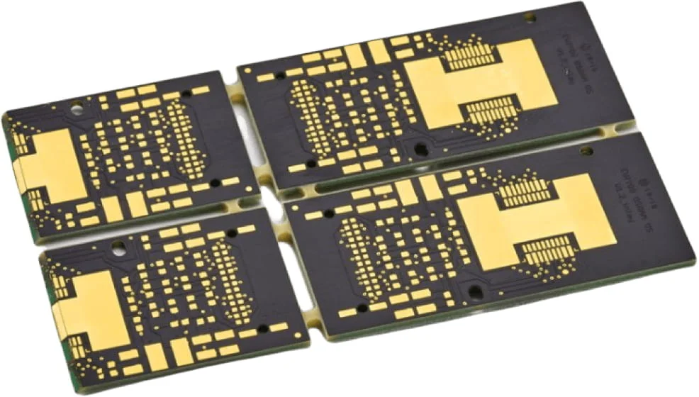
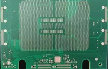
What is Multilayer PCB
Multilayer PCBs are printed circuit boards with 3 copper layers and above.
The core materials of multilayer PCBs can be FR4, aluminum, copper, PI, PET, PTFE, ceramics, etc. Components can mount on one side or both sides.
There are multilayer FR4 PCB, multilayer flexible PCB, and multilayer ceramic PCB. And rigid-flex PCB, HDI PCB, rigid-flex PCB, and high-frequency PCB belong to multilayer PCB.
To reduce the warpage, multilayer PCBs usually have a symmetrical structure. Typically, multilayer PCB has 4, 6, 8, 10, 12, or 16 copper layers.
At PCBONLINE, the wiring on multilayer PCBs is possible on up to 60 and 64 layers.
Multilayer PCB feature:
higher wiring densitysmaller product sizesmore circuit design flexibilityVia the ground and power layers, multilayer PCBs reduce EMI (electromagnetic interference)
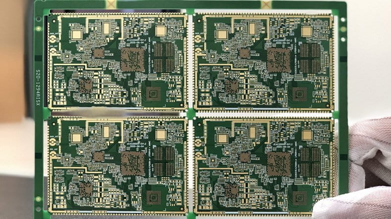
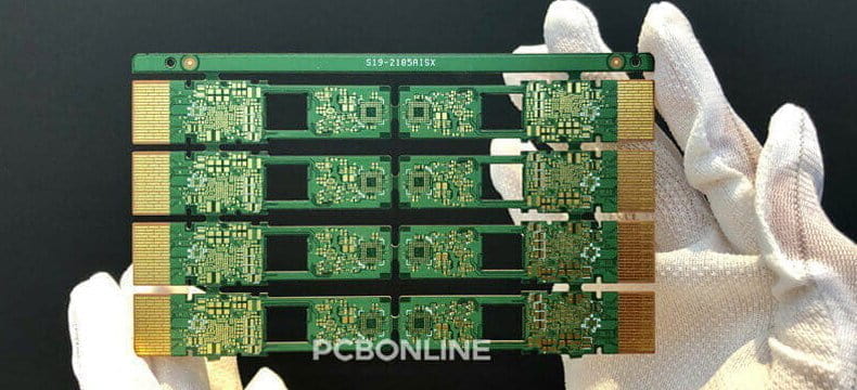
Multilayer PCB Manufacturing
The multilayer PCB manufacturing workflow is:
Cutting laminate > generating circuit in inner layers > lamination > drilling > copper plating > generating circuit in inner layers > automatic optical inspection (AOI) > solder mask and silkscreen > surface finish > profile > electrical test > final quality control > packaging.
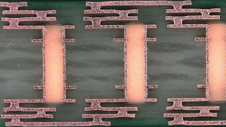
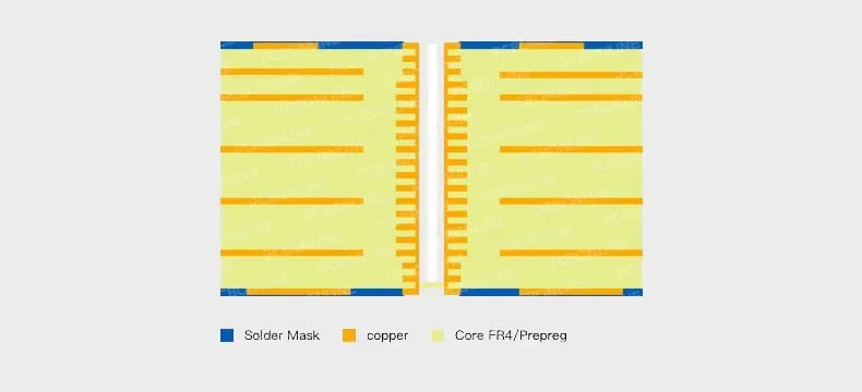
In multilayer PCB fabrication, the lamination process must have no air trapped in the board, the resin in the prepreg melts and cures and the two adjacent conductive layers are bonded and insulated.
Before generating circuits in the outer layers, on the inner layers, there should be an oxidation layer, which roughens the copper surface to integrate with prepreg.
If the oxidation is Cu₂O, we call the multilayer PCB manufacturing method the "brown oxid" process; if the oxidation is CuO, we call the method the "black oxide" process.
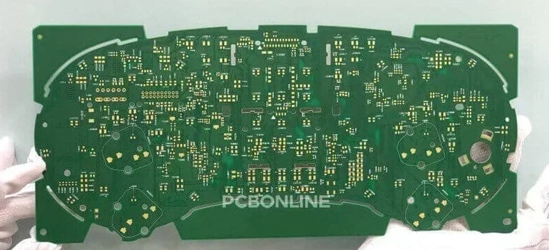
PCB Layer Quantity of Multilayer PCB
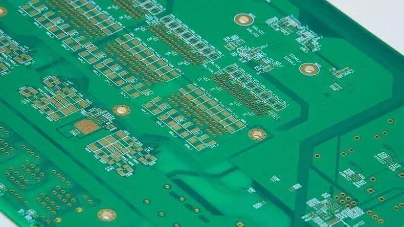
At the one-stop multilayer PCB manufacturer PCBONLINE, you can have any kind of multilayer PCB manufactured and assembled. The PCB layer quantity to fabricate is below:
FR4 multilayer PCB: 4-layer PCB, 6-layer PCB, 8-layer PCB, 10-layer PCB, 12-layer PCB, 16-layer PCB... 60-layer PCB, and 64-layer PCBCeramic multilayer PCB: 4-layer PCBRigid-flex PCB: 3-layer PCB, 4-layer PCB, 6-layer PCB, 8-layer PCB, 10-layer PCB, 12-layer PCB... 24-layer PCBFlexible multilayer PCB: 4-layer PCB, 6-layer PCB, 8-layer PCBHigh-frequency PCB: 4-layer PCB, 6-layer PCB, 8-layer PCB, 10-layer PCB... 24-layer PCB
If you need multilayer PCB prototypes and bulk production, you can send your Gerber to info@pcbonline.com to get a quote or chat online with PCBONLINE.
Multilayer PCB Manufacturing Capabilities
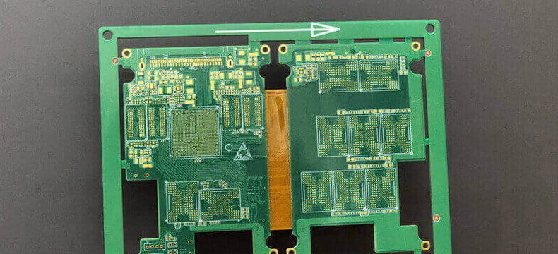
Applications of multilayer PCB:
computing, telecommunication, medical devicesindustrial controls, automotive equipmentdefense & aerospace systemsconsumer electronics, etc.
GET A FREE QUOTE
PCB and PCBA Certifications


Contact Our Expert Team Now

Learn about our products


Get customized services

 Phone
Phone WhatsApp
 Email
Email
Offer Electronics Manufacturing All-in-One
PCBONLINE® is a registered trademark or service mark of pcb online limited or its affiliates.
Copyright © 2005-2025 Pcb Online Limited. All rights reserved


