
4 Layer PCB Boards
A 4-layer PCB is a multilayer printed circuit board with the fewest circuit layers. Even though 4-layer PCBs are the most basic among multilayer PCBs, they are much more advanced than single or double-layer boards, because 4-layer PCBs allow the possibility of:
- more complex circuit design,
- 1+2+1 HDI capability,
- reduced space and more functions,
- better EMI shielding through the ground and power layers.
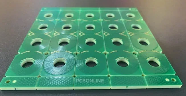
4 Layer PCB Manufacturing
![]()
For 4-layer PCBs, the second and third circuit layers are the so-called "inner layers". The two external copper layers are the outer layers.
4-layer PCB manufacturing begins with inner layers.
Let's look at the normal 4-layer FR4 PCB manufacturing process below.
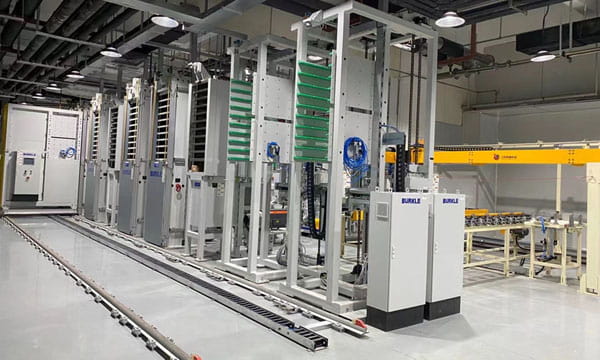
Step 1. Pre-clean the Copper Plate Laminates
![]()
FR4 copper plate laminates are composed of glass fiber epoxy resin covered by two copper layers. The two copper layers will become the second the third circuit layers of the 4-layer PCB in the next steps.
At first, the copper plate laminates are chemically cleaned to remove the protective coating, surface roughened, and coated with photoresist (so-called dry film) to prepare for circuit pattern imaging.
Step 2. Inner Layers Imaging (photoresist imaging)
This step aims to generate the second and third circuit layers on the copper plate laminate.
Above the copper plate, places the opaque PCB layout film which draws the transparent circuits.
The UV light irradiates the surface of the inner plate. Photoresist under the transparent film hardens and forms a protective film to the copper under it, while photoresist under the opaque film is still in the liquid state.
Then the liquid photoresist is washed away with chemical liquid.
Next, the exposed copper is etched away with sodium hydroxide (NaOH), while the copper under the hardened photoresist film is safe and sound.
Then the hardened photoresist film is peeled off. Now, the copper circuit is done, and the inner layers are finished.
Before the next lamination process, the inner layers are AOI tested to make sure the circuit is all right.
Step 3. Lamination
This step aims to layer up the two external copper layers on the inner plate. The two external copper layers will be the first and fourth circuit layers insulated from the inner layers by prepreg.
First, on the copper surface of the inner layers, we create an oxidation layer so that the surface is roughened and easy to integrate with prepreg. We call this process "brown oxide" if the oxidation is Cu₂O, or "black oxide" if the oxidation is CuO.
Next, the two alternating layers are layered up on both sides of the inner plate.
Then, under high temperatures and high pressure, the 4 layers are laminated without air trapped between them. The resin in the prepreg melts and cures and the copper layers are bonded and insulated tightly.
Step 4. Drilling and Electroplating Plated-Through Holes
4 PCB layers are electrically connected by PTH holes. First, the 4-layer board is mechanically drilled, and the excessive prepreg on the edges of the board is cut.
Then, the PTH hole walls are electroplated with copper. PCBONLINE already replaced the traditional electroplating baths with the VCP (vertical continuous plating) machine. The PTH holes' copper thickness of 4-layer PCBs at PCBONLINE is custom, from 1/3oz to 6oz.
Step 5. Circuit Generation on Outer (1st and 4th) Layers
Photoresist imaging on the two external copper layers is similar to that on the external layers, but the UV light hardens the non-circuit areas, and copper on the circuit areas is washed away.
Then the circuit area is electroplated with copper and then with tin, while the non-circuit area is insulated by the protective dry film and not electroplated.
Next, the dry film on the non-circuit area is peeled off. And the exposed copper is etched away by NaOH.
Then tin on the circuit area is removed. Now, only the copper circuit is left on the 4-layer PCB board.
Step 6. Solder Mask, Surface Finish, and Silkscreen
Solder mask is the protective film on the PCB surface, and surface finish is the protective film on the PCB pads.
Silkscreen is the symbol printed on the PCB surface when the solder mask and surface finish processes are completed.
At PCBONLINE, the solder mask color for the 4-layer PCBs can be green, red, blue, black, yellow, mink, brown, white, purple, or transparent. Solder mask types include line-to-pad and registration.
Surface finishes for the 4-layer PCBs can be HASL, lead-free HASL, ENIG, OSP, immersion tin, immersion gold, immersion silver, hard gold plating, peelable mask, and carbon ink.
Silkscreen color for the 4-layer PCBs can be white, black, yellow, blue, or red.
Step 7. Profile
The 4-layer PCBs are manufactured on a panel and they need to be separated. This step aims to treat the edge of the PCBs, such as half holes and v-cut.
Step 8. 4-Layer PCB Test, FQC, and Packaging
The basic tests for PCBs are electrical tests including the flying probe test and bed-of-nail test. If your 4-layer PCBs are used in the medical, automotive, aerospace, and defense industries, there is also four-terminal sensing to test the PCBs.
During and before the 4-layer PCB manufacturing, there have been tests to ensure solderability, PCB hole quality, electroplating copper, lamination, cleanness, and moisture absorption.
The above steps show how 4-layer PCBs are made. Apart from cost-effective 4-layer PCB manufacturing, the multilayer PCB manufacturer PCBONLINE provides 4-layer PCB assembly, electronic components for your boards, free DFM, DFT, and DFX, and one-on-one engineering support for your project.
4 Layer PCB Manufacturer
PCBONLINE is a reliable 4-layer PCB manufacturer and also one of the cheapest 4-layer PCB manufacturers.
Relying on advanced PCB manufacturing capabilities, PCBONLINE provides all types of 4-layer PCBs, such as rigid-flex PCBs, flexible PCBs, high-speed PCBs, 1+2+1 HDI PCBs, high Tg FR4 PCBs, etc.
PCBONLINE provides turnkey 4-layer PCB manufacturing and assembly without minimum order quantity limit, from prototyping to bulky fabrication.
Hear 4-layer PCB manufacturing comments from one of our customers who is an engineer:
"I have to say I'm quite impressed by the quality of work PCBONLINE guys have carried out! The paneling also came as a surprise to me and was beautifully done. I've also noticed that they do 4-layer boards at a price lower than most of their competitors."
Are you ready to start a 4-layer PCB project? You can contact PCBONLINE at info@pcbonline.com to get a quote.
Conclusion
4-layer PCBs belong to multilayer PCBs, and 4-layer PCB manufacturing is a lot more complex than single or double-layer PCB manufacturing. This article shows the whole 4-layer PCB manufacturing process step-by-step and also recommends a reliable and cheap 4-layer PCB manufacturer PCBONLINE.


