
High-frequency printed circuit boards (PCBs) find many applications in defense, communication, automotive, medical, and consumer electronics. However, high-frequency PCB manufacturing is highly demanding. To ensure the success of your high-frequency PCB and products, some critical factors are to be considered.
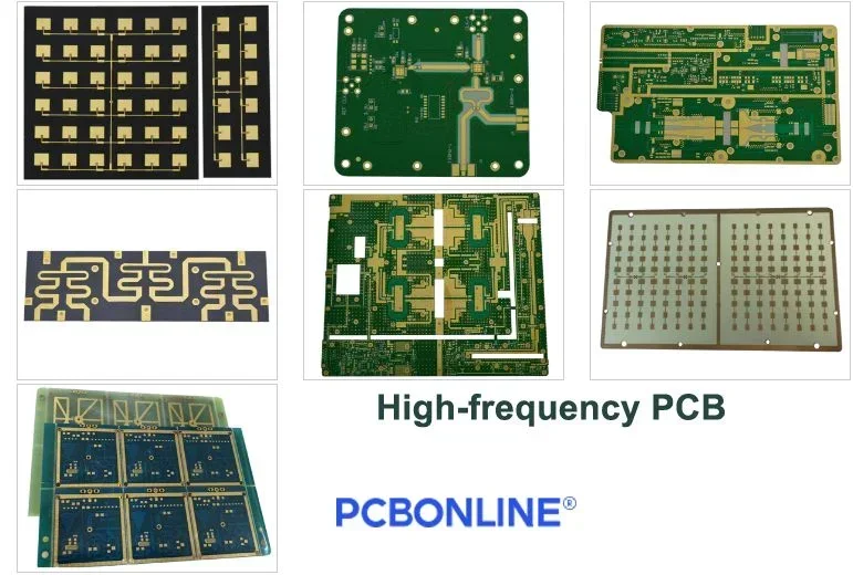
This blog reveals the top 3 key factors to consider in high-frequency PCB manufacturing. They are the Plasma process, confidentiality of the project, product, and customer information, and whether the PCB manufacturer has high-frequency laminate in stock or not.
Explore high-frequency PCB manufacturing from the below content.
Overview of High-frequency PCB
First of all, learn about what a high-frequency PCB is.
The printed circuits made using high-frequency laminates are high-frequency PCBs.
High-frequency PCBs transmit and receive signals of 300MHz and above (wavelength≤1m).
Microwave PCB (frequency ≥1GHz, wavelength≤300mm), and millimeter wave PCB (frequency of 26.5GHz to 300GHz, wavelength from 1mm to 10mm) belong to the high-frequency PCB range.
If the PCB materials are high-frequency laminates + FR4 laminates, the high-frequency PCB is a hybrid multilayer board.
If the PCB materials are high-frequency laminates + metal laminates, the high-frequency PCB is a high-frequency MCPCB.
High-frequency PCB Laminate Materials
High-frequency PCB laminates are much softer materials than FR4. The correct PCB materials ensure the functions and performance of the high-frequency PCB and product.
When choosing PCB laminates for high-frequency PCBs, consider the below factors.
1. Dk (Ɛr), dielectric constant, or relative permittivity
2. Df (tan δ), loss tangent, or dissipation factor
3. CTE, or coefficient of thermal expansion
They are supposed to be as small as possible.
Generally, the lowest Dk of high-frequency PCB materials is 2.17, and Df is 0.001.
Besides, high-frequency PCB materials should have low moisture absorption to avoid electrical performance deterioration in a high-humidity environment.
Additionally, the chemical and solvent resistance of the PCB material should be compatible with the technology used in high-frequency PCB manufacturing.
Applications of high-frequency PCB
The applications of high-frequency PCBs include but are not limited to:
Airborne and ground radar systems
Antennas
Power amplifiers
Live broadcast satellites
E-band point-to-point wireless communication link
Radiofrequency identification (RFID) tags
Millimeter wave applications
Missile guidance system
Space satellite transceiver
High-Frequency PCB Manufacturing
High-frequency PCB manufacturing is the same as normal FR4 PCB fabrication, and you can view the PCB fabrication process PDF at the end of this article.
However, circuit trace etching in high-frequency PCB manufacturing is very demanding.
High-frequency PCB etching requires the trace width tolerance to be +/-0.0007 inches and below.
After circuit generation, there's a 100x microscope to check the undercut and cross-section of the conductor.
Besides, the PCB manufacturer has careful management of the conductor's geometry and coating surfaces to avoid the skin effect.
No.1 Factor in High-Frequency PCB Manufacturing – circuit etching and Plasma process
Circuit generation includes copper etching, PTH (through-hole) drilling, and copper plating.
High-frequency PCB manufacturing requires no dust, gas bubbles, pinholes, or contamination on the copper and PTH walls.
Before etching, the PCB manufacturer uses an acid solvent to clean the copper foil surface to ensure no contamination.
Then the manufacturer grinds to roughen the copper foil surface and sprays a dry film coating on it.
After development and exposure, the non-circuit copper foil is etched away.
In drilling, the PCB manufacturer PCBONLINE uses the Plasma method to remove all the contamination from the PTH walls.
The principle of the Plasma method is that Plasma is highly active and can react with drill dirt and epoxy to eliminate them.
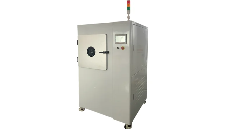
In the Plasma process, the high-frequency PCB is placed between two vacuum chambers. The high-frequency electromagnetic field is added to the two chambers to create the positive and negative poles.
Gases of CF₄, N₂, Oz, and Ar₂, are injected into the electromagnetic field and turned into the plasma.
After all the contamination is removed, the electromagnetic field is turned off and the plasma does not exist.
After the Plasma process, the high-frequency PCB is copper-plated immediately.
No.2 Factor in High-Frequency PCB Manufacturing – Confidentiality
High-frequency PCBs are high-performance boards widely used in military, aerospace, and other highly competitive industries. Keeping clients' information confidential is the duty of the PCB manufacturer.

Generally, you can sign an NDA (non-disclosure agreement) with the PCB manufacturer. The NDA is a legal file that demands the PCB manufacturer to keep confidentiality of all your information, including the entire PCB and product project and your company or institute's information.
The entire team of the PCB manufacturer PCBONLINE has received confidentiality training to ensure that clients' product and company information will not be leaked.
No.3 Factor in High-Frequency PCB Manufacturing – PCB Laminate in Stock
According to the manufacturing experience in the past 24 years, the time for high-frequency PCB manufacturing is affected by the sourcing of high-frequency PCB laminates.
Whether the PCB manufacturer has in-stock high-frequency PCB laminates matters for the delivery time.
With in-stock laminates, high-frequency PCB manufacturing can start immediately if the EQs (engineering questions) are clear.
If the PCB manufacturer has no high-frequency materials in stock for your PCB, the delivery time must be extended as it takes about 4 weeks to 6 months to purchase the required laminates.
Besides, for the sake of the quality of the in-stock laminates, the storage time must be within a period. This is because the PTFE laminate can absorb moisture after some storage time, affecting signal stability.
The PCB manufacturer PCBONLINE has in-stock high-frequency laminates of all brands and models, and their storage time is within 45 days to ensure the performance of the high-frequency PCB.
Besides, the other points of high-frequency PCB manufacturing include the below.
Surface finish in high-frequency PCB manufacturingThe surface finish for high-frequency PCB is suggested to be through chemical types, such as HASL (hot air solder leveling), ENIG, and OSP (organic solderability preservative). If it is the HASL, the PCB needs to be preheated at 150°C for half an hour, and it is 250°C to 265°C during tin spraying 3 times, each time lasting 3 seconds.
Testing the high-frequency PCBThermal shock is the testing method for the high-frequency PCB. It is a destructive test in high-frequency PCB manufacturing.
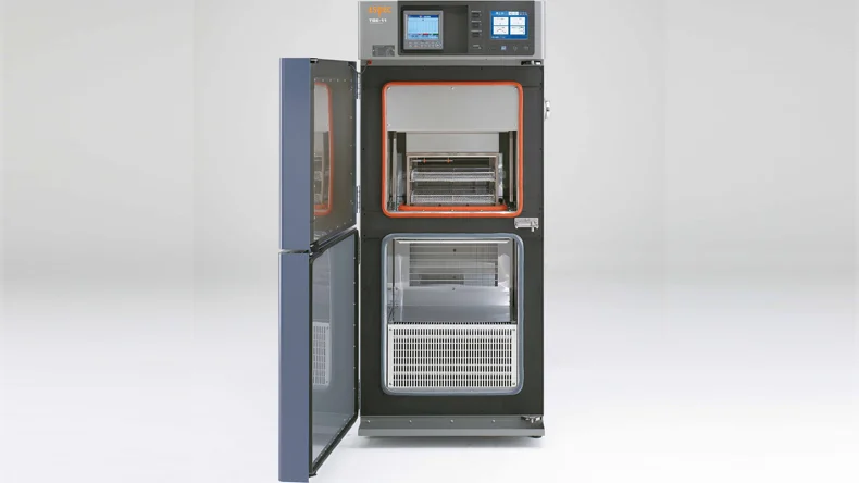
Thermal shock is at 288°C and lasts for 10 seconds each time. The times for thermal shock are 1 to 3 times according to different high-frequency PCB thicknesses, materials, and reliability requirements.
Protection of the high-frequency PCB
High-frequency PCBs can't be touched by hands throughout PCB manufacturing.
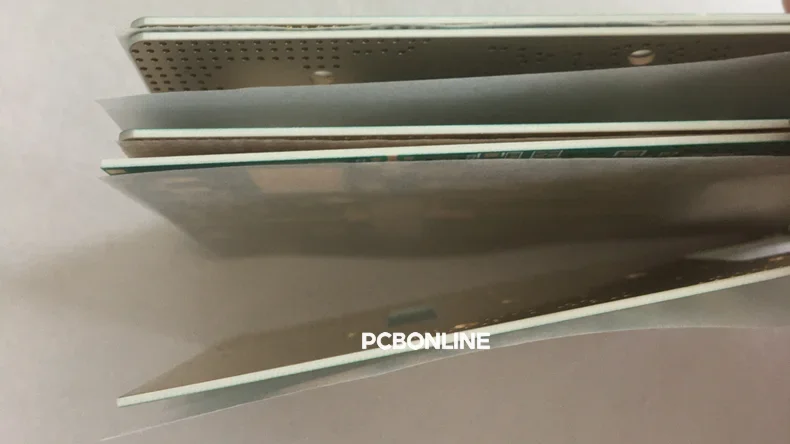
No scratches, pinholes, or pressing are allowed throughout the manufacturing and shipping.
For this, we lay down the high-frequency boards and separate each with paper during the transfer between different production lines and in shipping.
High-frequency PCB Manufacturer PCBONLINE
PCBONLINE has rich experience in high-frequency PCB manufacturing, engineering, and assembly. We keep the confidentiality of customer and product information.
If you need one-stop high-frequency PCB manufacturing and assembly, you can contact the one-stop high-frequency PCB manufacturer PCBONLINE.
PCBONLINE independently finishes the entire PCB manufacturing and assembly, including the etching, drilling, Plasma process, copper plating, surface finish, testing, profile, etc.
High-frequency PCB laminates within the 45-day storage period in stock of all brands, such as Rogers RO4000 series, RT5880, RT6006, Arlon Astra® MT, Taconic TLX series, etc.
High-frequency PCB manufacturing at PCBONLINE can be military and aerospace-grade from prototypes to bulk production.
All members of PCBONLINE have accepted confidentiality training. Your property, design, and your organization information are secure from leaking.
One-on-one engineering support throughout the project and PCBONLINE provides free samples for bulk production.
PCBONLINE has manufactured high-frequency PCBs and modules for many industries, such as defense, automotive, telecommunications, aerospace, medical, measurement, and consumer electronics. If you want to get a quote for your PCB or help in choosing high-frequency laminates or PCB design, contact PCBONLINE by email at info@pcbonline.com.
Conclusion
High-frequency PCB are high-reliability circuit boards used in middle and high-end applications, such as military and automotive. High-frequency PCB manufacturing is highly demanding, due to the precise impedance control, circuit etching, Plasma process, copper plating, and thermal shock for testing. Besides, the laminate stock matters for the delivery time, and the confidentiality matters for your project property and privacy. The PCB manufacturer PCBONLINE has expertise and is considerate of all factors in a high-frequency PCB and PCBA project. You can talk with PCBONLINE for any inquiry or question you have.
PCB fabrication at PCBONLINE.pdf


