
RF PCB is the abbreviation for the radio-frequency printed circuit board. It is a type of printed circuit board (PCB) designed to work with high-frequency signals, typically in the radio frequency (RF) range.
This blog not only explains the difference between RF PCB, microwave PCB, and high-frequency PCB. It provides an RF PCB design guideline and related content about RF PCB manufacturing.
Part 1: What is an RF PCB
RF refers to any frequency at which radio waves can be emitted, and the RF frequency range is 300KHz to 300GHz. RF PCBs are high-frequency PCBs that transmit radio-frequency PCBs. And they have an impedance of 50 ohms.
RF PCBs are typically made using specialized materials with low dielectric loss and high thermal conductivity. They employ controlled impedance and transmission line structures to maintain signal integrity. RF PCBs also include shielding and grounding features to reduce electromagnetic interference (EMI) and ensure reliable signal transmission.
RF PCBs are used in various applications, including wireless communication systems, microwave equipment, and radar systems. They are designed to minimize signal loss, interference, and noise, which can degrade the performance of high-frequency circuits.
Part 2: RF PCB vs Microwave PCB vs High-Frequency PCB
Apart from RF PCBs, you may also have heard about microwave PCBs and high-frequency PCBs. What's the relationship between RF PCB, microwave PCB, and high-frequency PCB?
All these PCBs are designed for high-frequency applications. Note that high-frequency PCBs contain RF and microwave PCBs, and RF PCBs contain microwave PCBs.
What are the differences between RF PCB, microwave PCB, and high-frequency PCB? See them below.
- Wave frequency definition: high-frequency waves are oscillating signals above 10KHz. Within the high-frequency range, there are the long wave, shortwave, super shortwave, and microwave. RF is the carrier frequency that a transmitter can emit, and microwaves have a wavelength from 0.1mm to 1mm.
- Frequency range: High-frequency PCBs operate wave signals above 10KHz, RF PCBs operate at the frequency range from 300KHz to 300GHz, and microwave PCBs operate at frequencies from 300MHz to 300GHz.
- Material: PCB materials are the substrate laminate and dielectric materials for the PCB. All these PCB materials require to have a dielectric constant (Dk), dielectric loss (DF), and thermal expansion and contraction as low as possible. High-frequency PCBs are made with materials like PTFE (Teflon), ceramic, or FR4. In contrast, RF PCBs are made with higher-grade PTFE materials like Rogers, and microwave PCBs use more specialized materials such as PTFE, PPO, and ceramic.
- Impedance: Impedance is the measure of opposition to an alternating current flow in a circuit. RF PCBs typically have an impedance of 50 ohms, while microwave PCBs may have an impedance of 50 or 75 ohms, and high-frequency PCBs may have an impedance of 50 ohms, 75 ohms, 100 ohms, or more.
To include it, microwave PCB takes up the "high frequency" part in the RF PCB range, and high-frequency PCB has a broader scope including RF PCBs and microwave PCBs.
Part 3: How to Design RF PCB
When designing an RF PCB, always remember to minimize signal losses, noise, and EMI, maximizing signal strength, stability, and bandwidth. Here's an RF PCB design guideline for your reference:
- Determine the design requirements: Before you start designing the RF PCB, determine the PCB's frequency range, power level, and impedance matching requirements. Also, decide what electronic components to use on the PCBA.
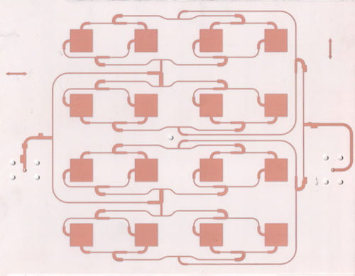
- PCB layout: Place components on the RF PCB in a way that minimizes the signal wire length and uses as few vias and turns as possible. And place smaller components around critical parts. Keep in mind to make the RF lines as short as you can and avoid routing them near high-speed digital traces, power planes, and other noise sources.
- Grounding: Provide a solid ground plane below the RF traces to minimize return paths and reduce crosstalk and radiation.
- Impedance matching: Use microstrip or stripline transmission lines to match the impedance of the RF traces to that of the components and connectors. Make sure the trace width and space meet the required impedance value and tolerances.
- Shielding: Use shielded connectors, metal cans, or RF shields to prevent RF signal leakage and reduce interference from external sources.
- Test: After the layout is completed, simulate and test to verify the performance of the circuit. Use a network analyzer or oscilloscope to measure insertion loss, return loss, and bandwidth.
- Optimization: Fine-tune the design to optimize performance by adjusting trace width, space, and length. Use electromagnetic simulation tools to analyze the RF behavior of circuits and optimize the placement of components.
Overall, designing an RF PCB requires careful planning and a deep understanding of RF design principles. By following RF design guidelines and using the correct tools and techniques, you can create reliable and high-performance RF circuits.
Part 4: A One-Stop RF PCB Manufacturer
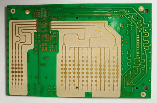
PCBONLINE is a one-stop RF PCB manufacturer located in Shenzhen. It is a source-factory manufacturer and provides fabrication and assembly for RF PCBs, microwave PCBs, and high-frequency PCBs from prototypes to massive manufacturing.
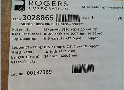
If you are looking for an RF PCB supplier to manufacture your design, pay attention to the laminates from the supplier, which are related to the delivery time and quality.
The success of RF PCB fabrication depends on the quality of laminates. The RF PCB laminates are softer than other PCB materials and the storage period is shorter. If the laminates are beyond expiration, they go bad, and the RF PCB using such laminates must fail. For this reason, most manufacturers only purchase RF PCB laminates when they receive an order. But it takes at least two weeks or even months to purchase the laminates, and you have to wait for a very long time.
But from PCBONLINE, you don't need to wait that long, and the RF PCB quality is guaranteed.
PCBONLINE always has high-frequency PCB materials in stock, such as Rogers, Taizhou Wangling, and Shengyi. The laminates are stored only within 45 days to ensure the best performance of the RF PCBs.
By working with PCBONLINE for RF PCB fabrication, you can enjoy many advantages:
- Fast RF PCB delivery and top quality due to in-stock high-frequency laminates within a storage period of 45 days.
- PCBONLINE manufactures RF PCBs to have a small impedance tolerance and optimized RF performances.
- It can make RF and digital interfaces on the same RF PCB without noise and interface with each other.
- PCBONLINE grasps the core technology to minimize thermal expansion and contraction of the RF PCB during fabrication and use.
- Besides, PCBONLINE can make embedded conductors and low-sensitivity antenna layers in the RF PCB.
PCBONLINE has many satisfied clients from research institutes and communications/automotive/defense application companies and business makers. If you need RF PCBs, no matter if you are in the early development stage or plan to enter the hardware building stage, you can always work with PCBONLINE for RF PCB fabrication, PCB assembly, and value-added services. Throughout your project, PCBONLINE provides free DFM and one-on-one engineering support. You can feel free to contact PCBONLINE by email at info@pcbonline.com.
Conclusion
RF PCBs belong to high-frequency PCBs and contain microwave PCBs. It is an advanced PCB to work with radio-frequency signals. Designing RF PCB should follow RF requirements in impedance matching, EMI shielding, grounding, etc. In RF fabrication, you also need to pay attention to the laminates quality of the supplier. By working with a reliable RF PCB manufacturer, you can have a successful RF PCB project designed and fabricated hassle-free, and you can start your PCBONLINE journey by chatting online from the chat window on the right.


