
![]()
Ceramic PCBs are composed of a ceramic substrate, a connection layer, and a circuit layer. Unlike MCPCB, ceramic PCBs do not have an insulation layer, and manufacturing the circuit layer on the ceramic substrate is difficult. How are ceramic PCBs manufactured? Since the ceramic materials were used as PCB substrates, quite a few methods were developed to manufacture the circuit layer on a ceramic substrate. These methods are HTCC, DBC, thick film, LTCC, thin film, DPC, and AMB. (in chronology)
HTCC
- Pros: high structural strength, high thermal conductivity, good chemical stability, high wiring density, RoHS-certified
- Cons: poor circuit conductivity, high sintering temperatures, expensive cost
HTCC is an abbreviation for high-temperature co-fired ceramic. It is the earliest ceramic PCB manufacturing method. The ceramic materials for HTCC are alumina, mullite, or aluminum nitride. Its manufacturing process is:
- At 1300℃-1600℃, ceramic powder (without glass added) is sintered and dried to solidify. If the design requires through holes, holes are drilled into the substrate board.
- At the same high temperatures, high-melting-temperature metal is melted as a metal paste. The metal can be tungsten, molybdenum, molybdenum, manganese, and so on. The metal paste is printed according to the design to form a circuit layer on the circuit substrate.
- Next, 4%-8% sintering aid is added.
- If the PCB is multilayer, layers are laminated.
- Then at 1500-1650℃, the whole combination is sintered to form the ceramic circuit boards.
- Finally, the solder mask is added to protect the ceramic circuit board.
Summary: as HTCC technology requires high temperatures, copper, silver, and gold can't be used for the circuit layer. The high-melting-point circuit metal has poor circuit conductivity. This leads to signal delay. So ceramic circuit boards made by the HTCC technology can't be used for high-speed and high-frequency circuits.
Instead, due to the features of high thermal conductivity and structure strength, HTCC ceramic PCBs are suitable for high-power microassembled circuits, high-reliability microelectronic integrated circuits, and vehicle high-power circuits.
DBC
- Pros: high thermal conductivity, high adhesion strength, excellent solderability, cheaper
- Cons: no through-holes, poor precision, rough surface, only applied to big-line-width design, only suitable for batch production
DBC is the abbreviation of direct bonded copper. It was invented in 1975. The copper-clad (thickness > 0.1mm) is directly bonded onto the ceramic substrate at high temperatures. The ceramic materials for DBC technology are alumina and aluminum nitride. Its manufacturing process is:
- In the N₂ atmosphere, the copper plate is directly bonded to the ceramic substrate at 1065℃-1083℃.
- Then the circuit layer is etched on the copper clad.
- If the PCB is multilayer, layers are laminated.
- Finally, a solder mask is added to protect the circuit.
Summary: During the ceramic PCB manufacturing process, there may be small bubbles between the ceramic substrate surface and the copper circuit layer. For this reason, the product's defective rate is high. And this technology doesn't allow through-holes to be drilled. If the design requires through-holes, ceramic PCB manufacturing has to adopt other methods.
However, DBC may be the cheapest and quickest ceramic PCB manufacturing method for batch production. There is no conspicuous connection layer between the ceramic substrate and the circuit layer, so the thermal dissipation is better.
Besides, the copper circuit layer has a high current-carrying capacity. A DBC ceramic PCB can reduce the module size and increase the power capacity. Due to these features, DBC ceramic PCBs are mainly used for packaging applications such as power electronic modules, semiconductor refrigeration, and LED devices.
Thick Film Ceramic PCB Manufacturing
- Pros: good mechanical strength, good surface flatness, high stability, RoHS-certified
- Cons: can't manufacture three-dimensional circuits, can't manufacture fine circuits, poor electrical conductivity
Unlike the above two ceramic PCB manufacturing methods, the thick film technology manufactures resistors while PCB manufacturing. The ceramic materials for thick film ceramic manufacturing are 96%/85% alumina (96% at PCBONLINE) and aluminum nitride. Its manufacturing process is:
- First, a circuit diagram is divided into many functional parts, and the parts are transferred into the planar circuit image on the ceramic substrate.
- Then a thick film circuit template is manufactured using the photoengraving method.
- At the same time, the thick film paste is prepared. The paste is manufactured by mixing fine metal (gold, platinum, copper, nickel, aluminum, or their alloy) powder, ceramic powder, and organic binder.
- Next, the thick film paste is printed onto the ceramic substrate using screen-printing technology.
- Then the thick film paste and the ceramic substrate are sintered to a whole at about 1000℃.
- During sintering, the organic binder decomposes and volatilizes, and the resistors also form.
- The resistors are trimmed by laser to the required resistance.
- Finally, a solder mask is added to protect the circuit.
Summary: the thick film technology can print the circuit with high precision on the ceramic substrate. But the circuit minimum line space of thick film ceramic PCBs is at least 60μm. So if the design has a line width smaller than 60μm, the circuit boards cannot be manufactured by the thick film method.
Besides, the circuit layer has poor electrical conductivity because of its ceramic/glass properties. For this reason, thick-film ceramic PCBs are manufactured for devices that have lower requirements for power and size.
LTCC
- Pros: high electrical conductivity, low dielectric loss, resistors can be printed during manufacturing, low sintering temperatures, manufacturing and assembly done together at one time
- Cons: unmatched contraction problems, thermal dissipation problems, lower thermal dissipation
LTCC is the abbreviation of low-temperature co-fired ceramic. It was invented in 1982. The ceramic substrate, components, and electrode materials are assembled when manufacturing. LTCC ceramic PCBs are usually multilayer and in three-dimensional design. The substrate materials for LTCC ceramic PCBs are glass-bonded ceramics, ceramic-glass composite, and glass ceramics. Its manufacturing process is:
- At lower temperatures, ceramic powder is sintered to be a dense raw ceramic substrate of precise thicknesses.
- Next, the raw ceramic substrate is drilled by laser.
- Then, liquid copper is injected into the vias, and precision conductive paste is printed to form the circuit layer.
- Passive components are placed between the multiple circuit layers, and then the circuit layers are laminated.
- At about 900℃, the whole structure is sintered to form a three-dimensional circuit board.
- Then solder mask is added to protect the circuit.
Summary: on the surface of the LTCC ceramic circuit board, ICs and active components can be assembled. In this way, LTCC ceramic PCBs can be manufactured to be passive/active integrated functional modules. The functional module can further miniaturize and increase the density. So LTCC ceramic PCBs are especially suitable for high-frequency communication devices.
Thin Film Ceramic PCB Manufacturing
- Pros: lower manufacturing temperature, fine circuit, good surface flatness
- Cons: expensive manufacturing equipment, can't manufacture three-dimensional circuits
The copper layer on the thin film ceramic PCBs has thicknesses smaller than 1mm. The main ceramic materials for thin-film ceramic PCBs are alumina and aluminum nitride. Its manufacturing process is:
- The ceramic substrate is cleaned first.
- In vacuum conditions, moisture on the ceramic substrate is thermally evaporated.
- Next, a copper layer is formed on the ceramic substrate surface by magnetron sputtering.
- The circuit image is formed on the copper layer by yellow-light photoresist technology.
- Then the excessive copper is removed by etching.
- Finally, the solder mask is added to protect the circuit.
Summary: the thin film ceramic PCB manufacturing is finished in vacuum condition. The yellow light lithography technology allows more precision to the circuit. However, thin-film manufacturing has a limit to copper thickness. Thin-film ceramic PCBs are suitable for high-precision packaging and devices in smaller sizes.
DPC
- Pros: no limit to the ceramic type and thickness, fine circuit, lower manufacturing temperature, good surface flatness
- Cons: expensive manufacturing equipment
DPC is the abbreviation of direct plated copper. It develops from the thin film ceramic manufacturing method and improves by adding the copper thickness through plating. Its manufacturing process is:
- The same manufacturing process of thin-film manufacturing until the circuit image is printed on the copper film.
- The circuit copper thickness is added by plating.
- The copper film is removed.
- Finally, the solder mask is added to protect the circuit.
Summary: DPC ceramic manufacturing can be planar or three-dimensional. PCBONLINE adopts the 3D DPC technology for ceramic PCB manufacturing.
DPC technology is appropriate for the manufacturing of most ceramic PCBs. Like thin-film ceramic PCBs, the lines are fine, and the circuit has high precision. 3D DPC ceramic PCBs are usually used for the three-dimensional hermetic packaging of high-power LEDs. Especially, the aluminum nitride DPC ceramic PCBs can be used for SiC/GaN-based optoelectronics and semiconductor power devices, optical fiber communications, 5G radio frequency modules, high-power microwave modules, photovoltaic modules, and MEMS sensors.
AMB
- Pros: strong bonding, good hot and cold cycle characteristics, fine circuit, good surface flatness
- Cons: expensive manufacturing equipment, can't manufacture three-dimensional circuits
AMB is the abbreviation of "active metal brazing". The AMB technology develops from DBC. Silicon nitride PCBs are fabricated mainly by AMB technology. AMB ceramic PCB manufacturing process is:
- In the N₂ atmosphere at about 800℃, active solder is silk screen printed on the ceramic substrate. The metal of the active solder is Ag/Cu mixed with Ti and Zr. Ti, Zr, and ceramic will form a reaction layer wettable by the solder.
- Then the ceramic substrate is clamped with oxygen-free copper clad and soldered in a Vacuum brazing furnace.
- The circuit is etched on the copper layer.
- Then electroless plating is conducted to the circuit pattern.
- If the PCB is multilayer, layers are laminated.
- Finally, a solder mask is added to protect the circuit.
Summary: Compared with DBC ceramic PCBs, AMB ceramic PCBs have stronger bonding and better hot and cold cycle characteristics. For IGBT used in high-power control modules, AMB ceramic PCBs are becoming a popular circuit board option. AMB ceramic PCBs currently are used in aerospace, electronic vehicles, and aviation fields.
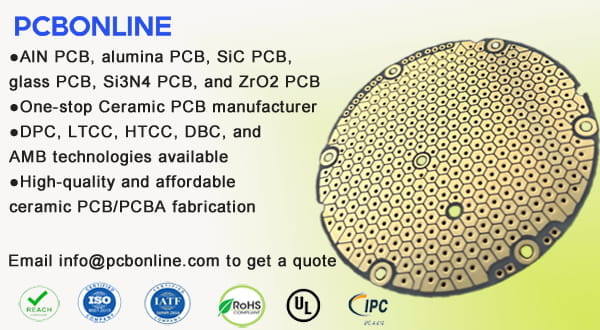
PCBONLINE: High-Quality Ceramic PCB Manufacturer
PCBONLINE, one of the leading ceramic PCB manufacturers, mainly adopts 3D-DPC technology for ceramic PCB manufacturing. HTCC, LTCC, DBC, and AMB are also available for ceramic PCB fabrication at PCBONLINE. PCBONLINE provides one-stop ceramic PCB manufacturing, PCB assembly, and box-build assembly, including alumina PCBs, aluminum nitride PCBs, SiC PCBs, IGBT modules, COB LED modules, ceramic LED plates, etc.
Here are some reasons to choose PCBONLINE as your one-stop ceramic PCB manufacturer:
- The copper thickness of the circuit layer is arbitrarily customized from 100nm to 300μm.
- Three-dimensional design and high density can be achieved.
- A better welding performance and temperature resistance.
- The circuit layer doesn't contain an oxide layer and has a longer shelf life.
- Maximum ceramic PCB size of 138mm × 190mm. For extreme prototypes, the max size is 160mm × 280mm. (Please leave a 4mm-5mm distance for the edge rails.)
- Ceramic thickness from 0.15mm to 4.0mm is available. (PCB thickness is 0.1mm more than ceramic thickness.)
- One-on-one engineering support throughout your project and free samples for bulk production.
PCBONLINE has rich experience in ceramic PCB fabrication and assembly for aerospace, automotive, aviation, laser, power, communication, and LED fields. We provide one-stop manufacturing from prototypes to bulk production. If you feel interested in having ceramic PCBs manufactured/assembled from PCBONLINE, feel free to send your inquiry by email at info@pcbonline.com.
Extended Reading: What to Pay Attention to in Ceramic PCB Assembly?
According to our experiences in ceramic PCB assembly, ceramic PCB SMT assembly differs from FR4 PCB SMT assembly.
The thermal dissipation capacity of aluminum nitride is much better than that of FR-4. Based on this, we suggest:
- Bake to preheat the AlN PCB before solder paste printing.
- After placing electronic components on the AlN PCB, the reflow soldering progresses. The furnace temperature of the reflow soldering should be higher than that of FR-4 and the speed of the PCB passing through the furnace should also be accelerated.
We hope the above technical information is helpful to you. In addition, the price of aluminum nitride has been lowered. If you place orders in 2023, the AlN PCB price will be lower than in 2022. Welcome to chat with us from the online chat window on the right.
Conclusion
This article lists the common ceramic PCB manufacturing methods. It introduces the ceramic PCB manufacturing processes and gives a brief analysis of the methods. If engineers/solutions companies/institutes want to have ceramic PCBs manufactured and assembled, PCBONLINE will bring 100% satisfying results to them.


