
For PCBs used for different applications, the maximum current allowed to flow through is different. Usually, the expected current of a PCB is within 10A. What's more, the PCB current for consumer electronics is usually within 2A. However, industrial, automotive, and other high-power applications require high currents to flow through PCB traces.
How do you design PCB trace widths and copper thickness for large-current applications? What is the relationship between trace width and PCB current? Any tips for high-current PCB design?
PCBONLINE, an EMS PCB manufacturer, provides contract manufacturing services for industrial, automotive, medical, defense, computing, and consumer applications. If you need one-stop PCBs with any trace width, copper thickness, substrate material, and power, PCBONLINE is a reliable PCB supplier choice that can help your project design. Here are 4 tips for high-current PCB design:
- Increasing the trace width and copper thickness.
- Choosing high thermal conductivity materialssuch as metal and ceramic for the PCB substrate.
- Using terminal blocks(also known as terminal connectors) on the PCB.
- Inlaying copper busbarsin the PCB substrate material.
In this article:
Part 1: PCB Trace Width vs Current Tables for Different Currents Part 2: Increasing Trace Width and Copper Thickness for High-Current PCBs Part 3: Using Terminal Block or Copper Busbar for High-Current PCBs Part 4: Custom Design and Manufacture PCBs of Any CurrentPart 1: PCB Trace Width vs Current Tables for Different Currents
First of all, here's the knowledge for your PCB design: increasing trace width, copper thickness, and thermal conductivity enhances the PCB's current carrying capacity.
So what exactly trace width should you use for PCBs in different currents? These two PCB trace width vs. current tables explicitly reveal the answer you're looking for!
Table 1. PCB Trace Width, Copper Thickness, vs Current at 10°C Temperature Rise
|
35μm
|
50μm
|
70μm
|
105μm
|
135μm
|
|
|
0.15mm
|
0.20A
|
0.50A
|
0.70A
|
/
|
/
|
|
0.2mm
|
0.55A
|
0.70A
|
0.90A
|
/
|
/
|
|
0.30mm
|
0.80A
|
1.10A
|
1.30A
|
/
|
/
|
|
0.40mm
|
1.10A
|
1.35A
|
1.70A
|
/
|
/
|
|
0.50mm
|
1.35A
|
1.70A
|
2.00A
|
/
|
/
|
|
0.60mm
|
1.60A
|
1.90A
|
2.30A
|
2.70A
|
/
|
|
0.80mm
|
2.00A
|
2.40A
|
2.80A
|
3.30A
|
/
|
|
1.00mm
|
2.30A
|
2.60A
|
3.20A
|
3.90A
|
6.30A
|
|
1.20mm
|
2.70A
|
3.00A
|
3.60A
|
4.40A
|
7.20A
|
|
1.50mm
|
3.20A
|
3.50A
|
4.20A
|
5.20A
|
8.50A
|
|
2.00mm
|
4.00A
|
4.30A
|
5.10A
|
6.40A
|
10.50A
|
|
2.50mm
|
4.50A
|
5.10A
|
6.00A
|
7.60A
|
12.30A
|
|
3.00mm
|
5.00A
|
5.50A
|
6.40A
|
8.60A
|
14.10A
|
|
4.00mm
|
5.40A
|
6.20A
|
7.90A
|
10.60A
|
17.30A
|
|
5.00mm
|
5.60A
|
7.30A
|
9.30A
|
12.50A
|
20.40A
|
|
8.00mm
|
7.90A
|
10.30A
|
13.10A
|
17.60A
|
28.70A
|
|
10.00mm
|
12.00A
|
15.40A
|
20.70A
|
33.70A
|
12.30A
|
Table 2. PCB Trace Width, Copper Thickness, vs Current at 20°C Temperature Rise
|
|
35μm
|
50μm
|
|
1.00mm
|
7.20A
|
8.60A
|
|
1.20mm
|
8.20A
|
9.80A
|
|
1.50mm
|
9.60A
|
11.50A
|
|
2.00mm
|
11.80A
|
14.20A
|
|
2.50mm
|
13.90A
|
16.70A
|
|
3.00mm
|
15.90A
|
19.10A
|
|
4.00mm
|
19.60A
|
23.50A
|
|
5.00mm
|
23.10A
|
27.70A
|
|
8.00mm
|
32.40A
|
38.90A
|
|
10.00mm
|
33.60A
|
45.80A
|
Need explanations of the terms in the tables?
A PCB is a laminated board that consists of prepreg/substrate material layers and copper layers. The currents flow only through copper traces. How large the current can flow through the PCB is determined by the resistance of the PCB traces. The copper trace resistance is determined by the trace width and copper thickness.
Copper thickness refers to the thickness of PCB copper traces that currents flow through, and we use oz or um as the unit of the copper thickness (1oz = 35um).
The trace width is the width of copper traces. We use mm or mil as the unit of the trace width (2.5mm=100mil).
As you can see, a larger trace width and copper thickness lead to a large cross-section of a copper trace.
The temperature rise refers to the difference between the highest temperature in a PCB and the ambient air temperature during operation. The larger temperature rise means the PCB dissipates thermal to the air more quickly. That is to say, a PCB with good thermal conductivity has a large temperature rise.
Substrate materials for high-current PCBs can be ceramic (including aluminum nitride, aluminum oxide, silicon carbide, and silicon nitride), glass, aluminum, and copper. If you use copper inlays or terminals, FR4 and PTFE that have poor thermal conductivity can also be high-current PCB laminate material. (You can check examples in Part 3.)
In PCB design, the length of PCB traces can be any, but the copper thickness and trace width are settled. So is the temperature rise when the PCB substrate material, component-mounting sides, PCB layers, and copper thickness are settled.
Part 2: Increasing Trace Width and Copper Thickness for High-Current PCBs
What copper width and trace width should be for PCBs with different currents?
For FR4 PCBs, flexible PCBs, rigid-flex PCBs, and PTFE PCBs, you can use the table with the 10°Ctemperature rise for reference. For ceramic PCBs, aluminum PCBs, copper-base PCBs, and glass PCBs, you can use the table with the 20°C temperature rise for reference.
If you want to design a 4.5A PCB, you can use a 2.5mm trace width and 1oz copper thickness, and the laminate material is the FR4.
If you want to design a 100A PCB, you can use a 15mm trace width and 4oz copper thickness, and the PCB can be ceramic or copper-based.
The below equivalent for PCB current can help you calculate more accurately:
∆T is the temperature rise. A is the cross-sectional area (trace width × copper thickness). 0.048, 0.044, and 0.725are coefficients that are gained by test data. You can check "How to Determine PCB Trace Width and Current" for details.
Besides increasing the trace width and copper thickness, what other methods can you use to improve the PCB's current carrying capacity?
Part 3: Using Terminal Block or Copper Busbar for High-Current PCBs
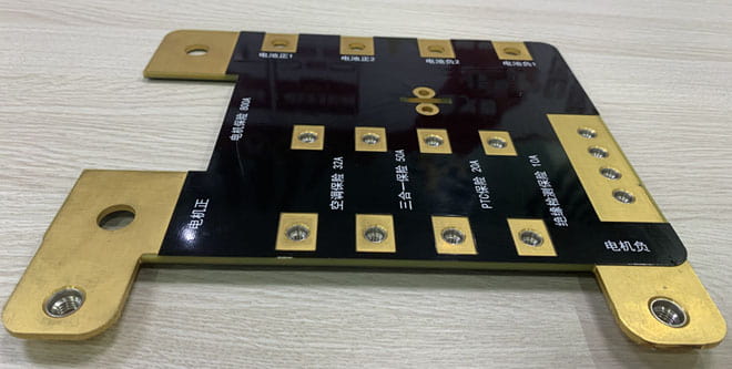
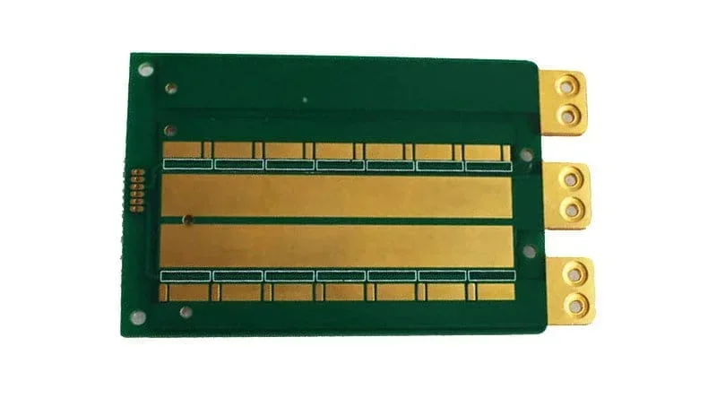
You can install terminal blocks (also known as terminal connectors), a kind of connector to attach a single wire that can withstand the expected current. For example, you can check the below high-current PCBA used for EV battery pack's cell contact system (CCS).
Screw terminals can be added to PCBs used for communications, medical, power, computing, and mobile applications.
What's more, you can inlay or mount copper busbars in the PCB substrate to increase the PCB's current carrying capacity. The PCB can withstand high currents because the high currents flow through the PCB busbar rather than the copper traces.
For example, you can check the below automotive PCBA manufactured by PCBONLINE. It is a high-power charging pile conversion board for fast-charging electronic vehicles (EV) and hybrid electronic vehicles (HEV).
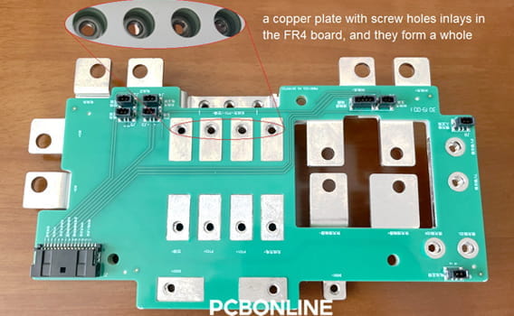
PCBONLINE has strong PCB/PCBA manufacturing capabilities and technical experiences for EV/HEV automotive electronics. In designing this high-current PCB, PCBONLINE separates the large and small currents. PCBONLINE uses copper busbars for large current conduction and thermal dissipation, and an FR4 PCB area with a 3oz copper thickness for small currents and signal conduction. Such a design ensures safety and reliability. The PCBA can quickly transfer heat when fast charging the EV's lithium battery pack.
Copper busbars are used on PCBs for ultra-high-current electrolysis and metal smelting, high/low voltage electrical appliances, switch contacts, power distribution equipment, busways, etc.
Part 4: Custom Design and Manufacture PCBs of Any Current
If you need cost-effective and high-quality electronics manufacturing services, you can choose PCBONLINE as your one-stop PCB manufacturer. PCBONLINE has two large advanced PCB manufacturing bases and one PCB assembly factory and provides source-factory PCB/PCBA manufacturing at a competitive price.

If you want to work on a project for automotive, industrial, defense, medical, communications, computing, and consumer electronics, you can work with PCBONLINE. No matter what the expected current and power of the PCB are, PCBONLINE provides considerate manufacturing services with one-on-one engineering support throughout your project.
Available PCB substrate: FR4 of any Tg, ceramic, polyimide, polyester, PTFE (Teflon), aluminum, copper, and glass.
Copper thickness: any copper thickness in the range from 1/3oz to 14oz
Trace width/space: 1.6mil/1.6mil and above
PCB layers: FR4 PCB 1 to 64 layers, ceramic PCB and aluminum PCB 1 to 4 layers, copper base PCB 1 to 8 layers, flexible PCB 1 to 10 layers, rigid-flex PCB 2 to 30 layers, transparent flexible PCB 1 to 6 layers, high-frequency PCB and HDI PCB 4 to 24 layers, and glass PCB 1 layer
Quality certifications: ISO 9001:2015, IPC, IATF 16949, RoHS, REACH, and UL
PCB quantity: 1 to 100,000+
Lead time: 8 working hours to 4 weeks based on fabrication complexity
PCBONLINE will check your Gerber carefully to make sure your design is feasible and help solve technical issues. For some applications, such as LED lights, if you order massive manufacturing, PCBONLINE can design the PCB and provide samples for you for free. Besides, you can avail of PCB assembly, component sourcing, and value-added services such as conformal coating and box build assembly from PCBONLINE. If you feel interested in PCB/PCBA fabrication from PCBONLINE, send your inquiry by email to info@pcbonline.com.
Conclusion
There are four large-current PCB design tips, and they are increasing PCB trace width and copper thickness, using high-conductivity substrate material, using terminals, and inlaying copper busbars. This article also provides the PCB trace width vs. current tables for different currents. So if you design either a high-current PCB or a low-current PCB, this article helps. In regards to PCB fabrication, the one-stop PCB manufacturer PCBONLINE is always there ready to work for you.
©This article is an original work of the PCBONLINE team. Please indicate the author PCBONLINE if you reprint. If the article is reproduced without permission or indicating the author's source, PCBONLINE reserves the right to investigate the infringement.
CCS Product Introduction - PCBONLINE.pdf


