
PCB copper thickness refers to the thickness of a circuit layer embedded in a printed circuit board. The higher the PCB copper thickness, the larger currents that can flow through the trace and the PCB can withstand. The common PCB copper thickness is 1oz, which equals 35μm. For PCBs used for high-current applications, you will need larger copper thicknesses for your PCB, and the PCB you design is a heavy-copper PCB.
What is Heavy-Copper PCB
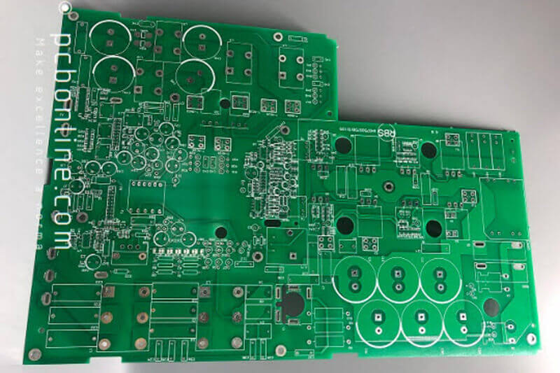
Heavy-copper PCBs are printed circuit boards with a 3oz and above copper thickness. Heavy-copper PCBs can withstand high electrical currents, and most of them are used for power equipment.
Though in theory, the copper thickness can be any by electroplating copper on the copper-clad laminates, we use heavy-copper PCBs with a copper thickness of 14oz (490μm) and below. That is to say, heavy-copper PCBs have a copper thickness range of 3oz to 14oz.
The larger the copper thickness, the larger the trace width/space. For this reason, heavy-copper PCBs usually have a simpler circuit design than many high-density PCBs.
The copper-clad laminates (CCL) for heavy-copper PCBs should be high-quality, and we can choose the Shengyi laminates, which have precise etching circuits with a smaller tolerance.
Heavy-Copper PCB Manufacturing
Heavy-copper PCB fabrication is different for different copper thicknesses.
For PCBs with a copper thickness smaller than 10oz, heavy-copper PCB manufacturing is etching the copper-clad laminates. The copper thickness of PCB copper-clad laminates is 1/3oz to 12oz.
For multilayer PCBs, the circuits of the internal layers are directly etched on copper-clad laminates, and the external layers are electroplated with copper to add to the required copper thickness and then etched to make the circuits.
For example, for a heavy-copper PCB with 3oz internal and external circuit layers, PCB fabrication is using the 3oz copper clad laminates for internal layers and 2oz CCL for external layers, and electroplating copper to add the external layer copper thickness to be 3oz, and then laminating the layers.
For the fabrication of heavy-copper PCBs with a 10oz and above copper thickness, the manufacturer doesn't use copper-clad laminates but red copper foil. In PCB manufacturing, we laminate copper foil with prepreg to manufacture heavy-copper PCBs.
In the solder mask step, silkscreen printing solder mask ink may cause uneven solder mask thicknesses. This is because the ink can accumulate in the circuit corners and around the PCB vias, and the areas without copper have a thin PCB ink thickness. The uneven solder mask on the board surface can't protect the copper in the PCB, and the anti-puncture performance is greatly reduced.
For this reason, the thick-copper PCB manufacturer PCBONLINE uses electrostatic spraying solder mask technology to replace the traditional printing solder mask process.
In the electrostatic spraying process, the PCB ink is directly and evenly sprayed on the surface of the board. The thickness of the ink on the entire PCB is uniform, and the board looks bright and achieves the best protection effect and the best appearance.
Heavy-Copper PCB Assembly
The heavy-copper PCB assembly process is the same as other PCB assemblies and also includes the SMT assembly and THT assembly. But according to our experience, reflow soldering temperatures for heavy-copper PCBs should be much higher than other PCBs.

We suggest the peak temperatures of reflow soldering for heavy-copper PCBs from 290°C to 300°C. As we know, the peak temperature range of lead-free PCB reflow soldering is 240°C to 270°C. Why does heavy-copper PCB require so much higher reflow soldering temperatures?
The reason is that much copper leads to quick thermal dissipation, and the copper pads of heavy-copper PCBs transfer heat quickly. The reflow soldering temperatures have to be much higher so that the thermal left on the copper pads is enough to melt tin in the solder paste. After many times of testing, we find that the reflow soldering temperatures of 290°C to 300°C achieve good wetting and soldering effect.
One-Stop Heavy-Copper PCB Manufacturer
PCBONLINE is a one-stop heavy-copper PCB manufacturer providing heavy-copper PCB manufacturing and assembly from prototypes to bulky production.
PCBONLINE is a source manufacturer having two advanced PCB manufacturing bases and one PCB assembly factory. The earliest PCB factory of PCBONLINE was founded in 1999, and the EMS factory of PCBONLINE has more than ten years of experience in heavy-copper PCBA fabrication.
The core competitiveness of PCBONLINE in heavy-copper PCB fabrication is the solder mask electrostatic spraying process mentioned above. We already replaced traditional solder mask printing with electrostatic spraying solder mask technology.
By working with PCBONLINE for your heavy-copper PCB project, you can enjoy these benefits:
- PCBONLINE can manufacture all kinds of PCBs with a wide copper thickness range from 1/3oz to 14oz.
- One-on-one engineering support throughout your project and professional assistance to optimize your design.
- Reduce your heavy-copper PCB project with the optimal PCB design without quality and functionality sacrifice.
- Free PCBA sample and functional testing for bulky production orders.
PHeavy-copper PCB and PCBA manufacturing from PCBONLINE is certified with ISO 9001:2015, IATF 16949, REACH, RoHS, and UL. You can have EMS manufacturing from PCB fabrication to box-build assembly from PCBONLINE. If you have a heavy-copper PCB project to have manufactured, feel free to send your inquiry by email at info@pcbonline.com.
Types of Heavy-Copper PCBs
Heavy-copper PCBs can be in any substrate materials, and they are FR4 heavy-copper PCBs, flexible heavy-copper PCBs, aluminum heavy-copper PCBs, ceramic heavy-copper PCBs, and Teflon heavy-copper PCBs.
FR4 heavy-copper PCB
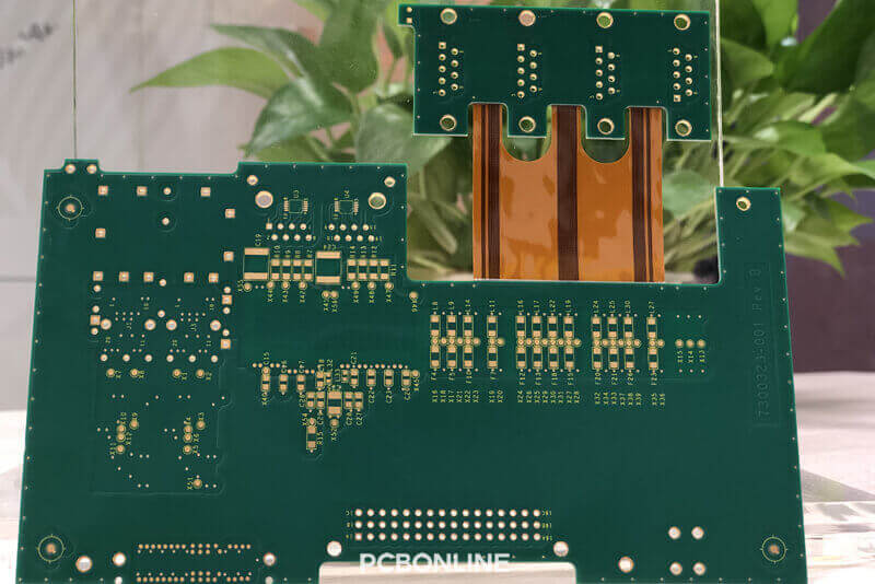
FR4 PCBs are the most common heavy-copper PCBs, and the copper thickness can be up to 14oz. And the PCB layers can be up to 24 layers. Both single and double component-mounting sides are available. For example, the FR4 PCB below is a 12-layer heavy-copper FR4 PCB with a 4oz internal and external copper layer thickness.
Ceramic heavy-copper PCBs
Ceramic PCBs include aluminum nitride PCBs, aluminum oxide PCBs, silicon nitride PCBs, silicon carbide PCBs, sapphire PCBs, and zirconia PCBs. Single component-mounting-sided ceramic PCBs are available to fabricate from PCBONLINE. The copper thickness of ceramic PCBs can be up to 4oz, and PCB layers are up to 4 layers.
Aluminum heavy-copper PCBs
From PCBONLINE, aluminum PCB manufacturing is automatic and the most affordable. The copper thickness ranges from 1oz to 6oz. And the PCB layers can be up to 4 layers. Both single and double component-mounting sides are available.
Flex heavy-copper PCBs
As we know, flexible PCBs are used to conduct signals rather than large electrical currents. But flex PCBs can also be heavy-copper. However, the copper thickness is up to 3oz. Otherwise, the flexibility is affected due to much copper. From PCBONLINE, flex PCB layers are up to 8 layers, and both single and double component-mounting sides are available.
Teflon heavy-copper PCBs
Teflon PCB, or PTFE PCBs, are high-frequency PCBs using Rogers, Taizhou Wangling, Nelco, or Taconic PTFE laminates. From PCBONLINE, single and double component-mounting sides are available to fabricate, and the PCB layers are from 4 to 24.
Heavy-Copper PCB Applications
Heavy-copper PCBs are mainly used for high-current applications such as high-power power supplies and motor circuits. Some applications of heavy-copper PCBs are:
Automotive electronics
Heavy-copper PCBs find applications in ignition coils and other high-current modules in classic automotive electronics. Automotive PCBs have high-quality requirements and fabrication should be traceable. A “PPAP level 3 required” report recording every process and specification is delivered to our client with the PCBs and a COC report. And our IMS system also keeps the source records.
Electronic vehicles and hybrid-electronic vehicles
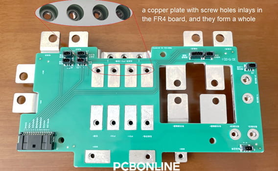
Due to the large currents and high power, charging the lithium battery module leads to much thermal, for safety and reliability, the PCB design separates the electricity networks of large currents and small currents. Copper plates conduct electricity and thermal for large-current circuits, and the PCB circuits with a 3oz copper thickness conduct electricity and thermal for small-currents. PCBONLINE is good at achieving a good combination of FR4 and copper plates on a PCB. The strong capabilities and technical experiences in electricity management for EV and HEV electronics will meet your demands.
High-power power supplies
Power supplies provide power to electrical appliances. High power and high currents are the work conditions for high-power power supplies. The circuits of a power supply don't have to be complex, but the copper thickness of PCB traces should be large so that large currents can flow through. Motors and engines usually use heavy-copper PCBs.
Medical equipment
Heavy-copper PCBs also find applications in medical appliances that require large currents, such as nuclear magnetic resonance equipment. Medical PCBs also have high-quality requirements. During PCB fabrication, PCBONLINE conducts four-terminal sensing to make sure the micro resistance is qualified for long-term uses.
Conclusion
Heavy-copper PCBs can be in any substrate material and the PCB copper thickness is 3oz and above. Heavy-copper PCB fabrication methods differ based on copper thicknesses, and the reflow temperatures for heavy-copper PCBs should be much higher than other PCB assemblies. If you need high-quality and affordable heavy-copper PCBs fabrication and assembly, the source factory manufacturer PCBONLINE won't let you down.
© This article is an original work of the PCBONLINE team. Please indicate the author PCBONLINE if you reprint. If the article is reproduced without permission or indicating the author's source, PCBONLINE reserves the right to investigate the infringement.


