Home>
Blog>
Solved - How to Determine PCB Trace Width and Current
Solved - How to Determine PCB Trace Width and Current
PCB trace
PCBONLINE Team Fri, Apr 02, 2021
17434
Question
I'm working on a project to create a PCB but I'm stuck on the question of how wide my traces need to be to accept the ~25-30A bursts. Right now the traces are 150mil on the top and bottom layer in most spots, will this be enough?
Current carrying capacity is the amount of current that flows in the PCB trace on continuous operation with an acceptable voltage drop. If the PCB traces are not designed for the current ratings required by the components, there could be burned-out traces, high voltage drops, and even a risk of fire due to heat generation in the traces. That's why you need to determine the PCB trace width and calculate its current when you design a high-current PCB.
Figure 01 - Burned PCB trace
In this article, we will discuss
how to determine PCB trace width,
current capacity, and
impedance you want to consider when designing a PCB.
How to Determine PCB Trace Width
The General current carrying capacity equation can be defined as:
Eq - 01 General currents carrying capacity formula
Where
I indicates the current in amperes,
∆T the change in temperature above ambient in °C, and A the cross-sectional area in mils. K, β1, and β2 are coefficients that are defined by test data.
For outside visible traces, the coefficient values are:
K = 0.048
β1 = 0.44
β2 = 0.725
And the equivalent current carrying capacity equation will be:
For outside visible traces the coefficient values are:
K = 0.024
β1 = 0.44
β2 = 0.725
By plotting the above equation for common temperature values, we can obtain the following chart.
Figure 02 - Current vs Cross-Sectional Area
By this chart, we can find what is the required cross-sectional area for a given current. After finding out the required cross-sectional area, there is another graph that can be used to easily find the required width of the PCB trace.
Figure 03 - PCB trace width vs Cross-Sectional Area
Eq -01 can be used for more accurate PCB designs. Temperatures above 100°C are not used because temperatures higher than 100°C can melt solder and damage components.
PCB Trace Width vs. Copper Thickness vs. Current
Here's a table telling you the relationship between PCB trace width, copper thickness, and current that can flow through the trace.
PCB copper thickness vs. trace width vs. current
Copper thickness 35um
Copper thickness 50um
Copper thickness 70um
Current (A)
Trace width (m)
Current (A)
Trace width (m)
Current (A)
Trace width (m)
4.5
2.5
5.1
2.5
6
2.5
4
2
4.3
2.5
5.1
2
3.2
1.5
3.5l
1.5
4.2
1.5
2.7
1.2
3
1.2
3.6
1.2
2.3
1
2.6
1
3.2
1
2
0.8
2.4
0.8
2.8
0.8
1.6
0.6
1.9
0.6
2.3
0.6
1.35
0.5
1.7
0.5
2
0.5
1.1
0.4
1.35
0.4
1.7
0.4
0.8
0.3
1.1
0.3
1.3
0.3
0.55
0.2
0.7
0.2
0.9
0.2
0.2
0.15
0.5
0.15
0.7
0.15
Table 01 - PCB trace width vs copper thickness vs current
In PCB design, you can follow the above table to set up the trace width and copper thickness according to the current requirements.
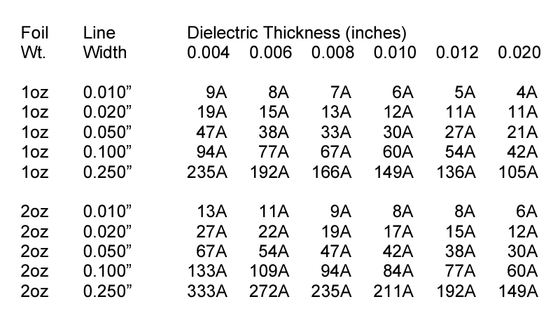
You can follow the figure below to select the appropriate PCB trace width and dielectric thickness for aluminum PCBs according to different copper thicknesses.
Figure 04 - Aluminum PCB trace width vs copper thickness vs dielectric thickness
How to Determine PCB Trace Current Capacity
There are two factors to be considered when sizing the traces of your printed circuit board (PCB). They are the current capacity of the trace and the impedance.
PCB trace materials, the cross-sectional area of the trace, and temperatures decide the current carrying capacity of copper traces.
The cross-sectional area of the trace is directly proportional to the current capacity. More cross-sections mean there is more surface area and more surface area helps to dissipate the heat which also increases current carrying capacity.
Choose PCB Trace Material Fit for Your Design
PCB trace material plays a vital role in determining the current-carrying capacity. Low-resistivity materials, such as silver, copper, and gold, have high current-carrying capacities. Copper (Cu) is the widely used PCB trace material that provides the best performance per cost. Gold or Silver plated copper traces are used in high-frequency digital signal processing PCBs. Gold is plated to avoid corrosion of copper traces.
Figure 05 - Gold-plated copper traces
The following chart provides the resistivity of materials that are used in electronic manufacturing.
Material
Resistivity at 20°C
Usage
Silver (Ag)
1.59×10^−8
Plating material to protect copper from corrosion and improve resistivity
Copper (Cu)
1.68×10^−8
Copper wires, traces, and alloys
Gold (Au)
2.44×10^−8
Plating material to protect copper from corrosion
Aluminum (Al)
2.65×10^−8
Aluminum wires, traces, and alloys
Table 02 - Resistivity
In a PCB, due to manufacturing limitations, the thickness of the copper trace is the same throughout the PCB and only the width is variable. In many cases, increasing the width of the trace is enough to achieve the required current rating. However, in some situations, there is not enough room to increase the width of the traces in the PCB. In such cases, the thickness of the trace is increased by applying solder on top of the trace.
Figure 06 - Solder on PCB traces
Operating Temperature Can Influence PCB Trace Resistivity
Operating temperature is another key factor when determining the dimensions of the PCB trace. As mentioned in Table 02, the resistivity of conductive material changes with temperature. Standard resistivity values are measured for 20°C. So every 1°C increase in temperature, the resistivity of the material will be increased by some amount. This change has to be compensated in the calculation for the PCB trace width.
The current carrying capacity of a trace also depends on the physical arrangement of the trace. For example, the same cross-section area outer trace has a higher current carrying capacity than an inner layer trace. This is due to that outer layers have better heat dissipation and hence can support more current.
As described above, many factors have to be considered when calculating PCB trace width for the required current capacity. Fortunately, there is a Standard defined to do this calculation quickly and accurately. IPC 2221 is a little bit older standard which was developed by data from 1954. The new standard which is IPC-2152, named "Standard for Determining Current Carrying Capacity in Printed Board Design", defines useful charts and calculations that can be used to design PCBs more accurately.
How to Control PCB Trace Impedance
Impedance is the second key factor that has to be considered after the current carrying capacity when designing a good PCB layout. Since most of the circuits are designed assuming PCB traces have little to no impedance, it is desirable to have impedances of the traces as low as possible.
Impedance is denoted by Z. It is the vector sum of resistance and reactance. It is an important parameter in high-frequency circuits. Since the reactance is proportional to frequency, impedance also increases with the working frequency.
Figure 07 - Impedance
The impedance of a PCB trace depends on trace length, spacing, cross-sectional area, current signal frequency, outside magnetic interference, trace’s self-inductance, trace material, solder material and quality, vias, and dielectric material between traces.
Instead of calculating impedances, designers follow a set of design practices that can reduce PCB impedances to an acceptable tolerance value:
Use the ground plane
Use PCB traces as short as possible
Use adequate trace spacing
Use traces of the same length
Avoid sharp turns in traces
Use turns in a minimum amount
Have PCB Manufacturered at PCBONLINE
When you're done with PCB design, it's time to ask a good PCB fabricator to turn your design into real boards. PCBONLINE, an advanced circuit board one-stop manufacturer, is ideal for you to work with. High quality is ensured by their two large advanced PCB factories and one assembly factory. You can enjoy free complete PCBA samplings for batch production, as well as extremely fast prototyping, free design for excellence, and tech support from a one-to-one engineering professional.
PCBONLINE's capability:
Layer: 1 ~ 42
Laminate: normal Tg/high-Tg/lead-free/halogen-free