
Question: I'm trying to create a PCB using AutoDesk Eagle but I am new to PCB designing. Is there any free guide to help?
Before we reveal the process of creating a printed circuit board with AutoDesk Eagle we should first see how the software works. Eagle's UI consists of several major interaction points including Library, Board, Schematic, and Control Panel. The library allows you to manage and edit parts, as far as the schematics where you draw the essential connections for a certain PCB. The board is where you lay out all the electronic components that are defined to be physically connected to the board. The control panel we will review separately as it is one of the most important features of the software.
Step 1: AutoDesk Eagle Control Panel
The control panel remains the most important aspect of Eagle's UI and it is the main window in the software. Once closed, all related windows that it opened within will close as well. The control panel contains various categories:
Design Rules (.dru) are an inbound feature for checking the rules of a certain PCB design.
Libraries (.lbr) are used for the software to store individual parts that you insert into your project.
User Language Programs (.ulp) are most commonly used for advanced scripting to assist with more complex designs and it is pretty much impossible without it.
CAM Jobs (.cam) is used to export to different formats.
Scripts (.scr) are essential groups of AutoDesk Eagle commands used for the execution of a certain command.
Projects - (.pcb, .sch, etc) is where your printed circuit board schematics or whatever you are doing is stored.
To create a new project for a printed circuit board, start by right-clicking on the "eagle" and selecting "New Project". Then you will have to download a "Compass.pcb" from the options listed below and save it in Documents\Eagle\ex-Compass. If files are still not appearing in the Control Panel, simply hit "F5" to refresh and they should pop out.
Once ready select your .pcb schematic and double-click it to load it into the software memory.
Step 2: AutoDesk Eagle Schematic Window
![]()
Once you are familiar with the Control Panel, it is time to explore the schematic window. This is where you can create and edit your printed circuit board schematic.
If you have never used AutoDesk Eagle before, you can start by learning how to move and control the schematic.
There are several different ways to move in Eagle, for instance, you can do that with button 1 on your mouse, or with the "F#" keys on your keyboard, and even zoom in and out with the scroll bar. The schematic window provides you with complete freedom of a point of view, angle, and many other beneficial aspects.
Use the mouse's middle button to move around and the middle click to pin. To zoom in and out simply scroll back and forth. You can also use the F# keys, F3 to zoom in, F4 to zoom out and F5 to center the screen focusing your cursor.
Step 3: AutoDesk Eagle Board Window
![]()
In the board view window, you can move and explore the board the same way as in the schematic window, so we won't go over that again. The display functionalities are the same, except for the view of the different layers. By default, you will be seeing them all at once, but you are allowed to isolate each of them. We will cover everything about the Board Window later in the process.
Step 4: Learn AutoDesk Eagle Definitions
Here are some of the general definitions that you need to understand before creating your printed circuit board in AutoDesk Eagle:
- Part - The part is a physical component on the printed circuit board, contained in the library.
- Trace - The trace is essentially a wire on the printed circuit board, used to create connections that Nets usually define.
- Net - The net is an electrical connection.
- Wire - Wires are used for cosmetics in the schematic view or plane modifications in the Board View.
- Label - Shows the name of a certain net.
- Plane - The plane is typically connected to the ground for high-current-carrying cases. With a Plane, the Eagle defines the border and the Plane will fill in as much surface/area as possible leaving room only for the traces you have bound inside.
- Value - This is the value of a certain part. In most common places the value is presented in complex numbers or the actual value for simpler parts like capacitors and resistors.
- Name - Identifies each part by name.
Step 5: Create a New Project
![]()
To start creating your first printed circuit board in Autodesk Eagle, follow the below-listed steps to create a new project before everything else.
1. Create a new project by clicking "File" > "New" > "Project".
2. Provide the project with a descriptive name.
3. Right-click on the newly created project and click "New" > "Schematic".
4. Provide your new schematic with a name as well.
Step 6: Add Parts to the Schematic
![]()
To insert the required parts for the project in the schematic click on the "Add" button and select the parts that you are going to use.
Step 7: Add Contention Between The Parts
![]()
Once you are ready to integrate parts in the schematic, it is time to make the connections. You can simply do that using the "Net" command. Do not use the "Wire" command to create connections, as we already mentioned that it is just for cosmetic add-ons on the schematic and they won't do anything. The best use for the "Wire" command is to illustrate something to check out how it looks and if it will work.
Here is some quick advice for using the "Net" command:1. Start netting with a single click, avoid double-clicking or dragging to start.
2. You can start anywhere.
3. After you start netting it will continue being drawn until you single click to pin in a spot.
4. A single click after you are already dragging the net will anchor it at the current cursor spot.
5. Right-clicking will instantly change the way that the net will go from point A to point B. The recommendation here is to use a 90-degree-angle form for easier netting in the schematic layout.
Step 8: Name and label the Nets
Use the "Label" command to name each of the nets easily and they will show up in the wire. Once all of the names are visible you can easily use the "Name" command to provide the wires with meaningful names that will help other engineers to easily navigate and understand that schematic board.
Here is why it is important to label & name the nets:
- It helps every time you decide to re-configure your schematic wiring. Without accurate labels, you will have to visually track each wire to see where you are disengaging it from.
- Provides a clear view to anyone who looks at the schematic or at least a basic understanding of how the components are wired.
Step 9: Provide Parts With Value
Use the "Value" located near the "Name" command to label all capacitors and resistors with their appropriate value. It is important to keep everything organized as inappropriate naming can result in a messy schematic. After all, navigating around the board nets is an activity all engineers go through multiple times per session so the rightful value will contribute to the overall process.
Step 10: Check Electrical Rules
![]()
AutoDesk Eagle has its functionality for checking where you have messed up. By running an Electric Rule Check (ERC), the software will examine the output of your printed board and determine if there are any issues.
Here are some of the common errors that you might experience on your very first ERC check.
- Unconnected Input Pin - Having an unconnected input pin is bad, but if the CON pin is a reference voltage that you can manually set, nothing bad will happen if you leave it like this (floating).
- Errors (n) - These errors are important to pay attention to. Anything here could be a reason for your printed circuit board to malfunction or even blow up after production.
- Warnings (n) - The warnings are not as urgent and dangerous as the errors but they surely require some of your attention. Most of the time warnings can appear if you haven't connected nets on both ends.
- Power Pin - With this warning, Eagle underlines that you have connected different voltages of power there. For instance, if you connect a 5V power supply line to a 12V power supply line bad thighs can happen. But if it is a really small difference you can leave it as it is.
- Part (n) Has No Value - This is one of the most simple errors that you can stumble upon and as its name suggests, you've forgotten to add a value to a certain part.
Step 11: Board Layout
![]()
Once you have the schematic and parts connections ready it is time to export the project in board view by "File" > "Switch to board". It will warn you that there is no board existing and you should click "Yes" to create a new board based on your schematics.
Once the board is created you will be able to see all parts on the left that are in use. You won't be able to drag out any parts from the board box area and even if you try, AutoDesk Eagle will refuse to cooperate.
Now it is time to set locations for all parts that they need to go just like connectors. It is recommended to group all parts that logically make sense together and move these cluster groups altogether to achieve as little amount of crossed unrouted lines as possible. Make sure to move all parts far enough apart that you don't break any design rule and also meet at least the minimum of unrouted traces crossing.
Step 12: The Other Side of The PCB
As we know printed circuit boards have a bottom side that requires your attention as well. To get a view of the bottom part use the "Mirror" command and click on the surface-mount parts to switch them on the bottom later. You might need to use the "Move" or "Rotate" command to orient the parts in their rightful positions.
Step 13: Route The Parts
![]()
To route the parts use the "Route" command and click on any airwire. This way a blue trace will appear at the node of the airwire that is the closest to your click. On the other hand, if a red trace appears this is not what we want and the workaround is to change the layer TOP (red) to BOTTOM (blue). Click again on some other place to anchor a wire on this spot, right-click to change the angle's turn, or middle-click to create a via between the bottom and the top layer until it is all blue.
Step 14: Check The Design Rules
There is an integrated Design Rule Check (DRC) that will ensure that the board you design is following all rules and has no errors. However, do not disappoint if a lot of common mistakes are found, instead try to resolve them. It is completely normal to encounter many mistakes on the DRC check.
Some of the common mistakes that you can encounter are mainly related to distance, clearance, size, and shape. We will reveal some of the common tabs that you will have to fulfill for a proper DRC check execution:
- Clearance - This prompt provides the software with information regarding the room you want between the different types of electrical connections on the board.
- Distance - This is the distance from any routing to the very edge of the printed circuit board.
- Size - You can set the minimum size and width that you desire and the DRC check will find anything that is not as determined.
- Restring - Generally it controls the size of the through-hole vias/pads, and the recommendation here is to leave it by default.
- Shapes - This will allow you to create pads with rounded edges, which you should leave by default as well.
After you fulfill everything required the right way, click "Check" and you will see the DRC Results. The fewer issues you see the better. Resolve issues and scan again until you have eliminated all the errors. In most cases, manufacturers fulfill all the printed circuit board design requirements and via DRC check they ensure that everything with the currently designed prototype is as per the customer's requirements.
High-Quality PCB Board Manufacturing
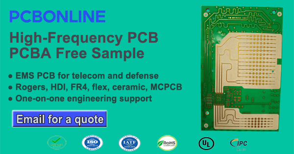
Once you have finished with all the routing and have no DRC errors the printed circuit board should be completed. You may be looking for a reliable PCB manufacturer. PCBONLINE, a one-stop advanced PCB manufacturer since 1999, is highly recommended for engineers and makers. You can get one-to-one free technical support from PCBONLINE about your project, free samples for batch PCB production, and free design for manufacturing and excellence. This PCB printing company can also assemble your boards and source all electronic components on your bill of materials. Working with PCBONLINE, you can realize your idea perfectly.
PCBONLINE's PCB manufacturing capability:
- Layer: 1 ~ 42
- Laminate: normal Tg/high-Tg/lead-free/halogen-free
- Surface finishing: OSP/HASL/LF HASL/immersion ENIG/immersion tin/immersion silver
- Board thickness: 0.15 ~ 3.2 mm
- Max board size: 500 × 580 mm
- Copper thickness: (inner finish copper) 1-4oz, (outer finish copper) 1-7oz
- Min. line width/spacing: 0.0635 mm/0.0635 mm
- Min. CNC drilling size: 0.15 mm
- Min. laser drilling size: 0.075 mm
- HDI stack up: 1+N+1, 2+N+2, 3+N+3
Last thing
The rendering could take up to 6 hours and even more on complex projects. Don't forget to contact PCBONLNE to check your Gerber free of charge and request a quote from them.


