
The breakneck speed of technological advancements is triggering an unmatched need for intricate and effective printed circuit board (PCB) designs.
Be it a veteran engineer or a greenhorn in the field, having potent PCB design tools at your disposal is indispensable for crafting complex, high-performing, and dependable circuit boards.
This blog offers a deep dive into the leading 5 free PCB design tools available in 2023, revealing their special advantages and competencies that distinguish them from the rest.
By scrutinizing the pros and cons of each software, our goal is to offer you priceless insights to help pick a proper PCB design tool for transforming your concepts into reality and securing success.
PCB Design Tool #1: EasyEDA
EasyEDA, a free web-based PCB design utilization, boasts a user-friendly and intuitive interface. This PCB design tool offers a straightforward and intuitive interface, including features for schematic capture, PCB layout, and simulation capabilities.

EasyEDA is particularly suitable for hobbyists and beginners due to its user-friendliness and extensive online component libraries. However, it might lack some advanced features needed for more complex designs.
Here's what EasyEDA brings to the table:
- Schematic capture: EasyEDA's sturdy schematic capture tool paves the way for the effortless design of circuit schematics. It delivers a user-friendly interface with drag-and-drop capabilities, simplifying the process of placing and connecting components.
- Component library: A vast component library in EasyEDA includes an array of pre-built components and footprints. This makes it a breeze for users to search and select components, freeing up time for focusing on design. The tool also allows users to create or import their own libraries.
- Simulation and analysis: With simulation and analysis features built into EasyEDA, users can confirm the performance and functionality of their designs. It supports a range of simulation types, such as transient analysis, AC analysis, and DC sweep, enabling users to study circuit behavior and refine their designs.
- Collaboration and sharing: EasyEDA offers embedded collaboration features that foster teamwork and sharing. Users can work with team members in real time, share designs, and offer feedback, promoting effective communication and making the design review process smoother.
- Community resources: The active user community of EasyEDA actively shares projects, tutorials, and design resources. Users can tap into a trove of community-contributed designs, libraries, and examples. Additionally, users can reach out to the online forum where the community offers help and guidance for any hurdles faced.
- EasyEDA API: EasyEDA offers an API, which lets users expand the tool's functionality and integrate it with other third-party software and services.
PCB Design Tool #2: KiCad
KiCad EDA is an open-source PCB design software suite catering to electronic design and PCB layout. Its open-source nature allows for customization and extension. It offers a full-fledged set of tools for schematic capture, PCB layout, component footprint creation, and more.

KiCad is celebrated for its robust features, versatility, and engaged user community. It has a steeper learning curve compared to EasyEDA but offers more advanced capabilities.
Here's a snapshot of KiCad's features:
- Schematic Capture: KiCad's user-friendly and flexible schematic capture tool lets engineers design complex circuit schematics. It supports hierarchical designs, making it a fitting choice for projects of different sizes and complexities.
- PCB Layout Design: The tool comes with a powerful PCB layout editor that empowers users to design multi-layer PCBs with advanced routing capabilities. It supports interactive and manual routing, differential pairs routing, and auto-routing options.
- 3D Viewer: KiCad's 3D viewer lets users visualize the PCB in three dimensions. This feature helps in spotting potential mechanical conflicts and ensures the proper fit of components on the board.
- Community support and libraries: KiCad benefits from an engaged and supportive user community. Users can access a large library of community-contributed schematic symbols, footprints, and 3D models, simplifying the process of finding and reusing components in their designs. The community proactively maintains and updates these libraries.
- Design rule checking (DRC): KiCad integrates a DRC feature that checks the design against user-defined design rules. It helps confirm that the PCB layout adheres to constraints such as minimum trace width, clearance between components, and clearance to the board edges. DRC helps in pinpointing potential errors or violations that might impact the functionality or manufacturability of the design.
- Gerber file generation: KiCad enables users to generate Gerber files, the industry-standard format for PCB fabrication data. Gerber files carry information about copper traces, pads, solder masks, and other PCB layers. These files can be forwarded to PCB manufacturers for fabrication.
PCB Design Tool #3: Fritzing
Fritzing is an open-source PCB design software tool that aims to support the design and documentation of electronic circuits, primarily catering to beginners and non-engineers.

This PCB design tool mainly targets electronics enthusiasts and focuses on creating interactive prototypes and documenting projects. It's great for breadboarding and prototyping.
However, Fritzing might lack some advanced features needed for complex PCB designs, and its development pace is slower compared to other tools.
Here's what Fritzing has to offer:
- Breadboard view: Fritzing presents a breadboard view that enables users to virtually assemble electronic components on a simulated breadboard. This view imitates the physical placement of components and their connections, making it convenient for users to prototype and tinker with circuits sans actual components.
- Educational material and tutorials: Fritzing provides an array of educational materials and tutorials to aid users in understanding electronics and circuit design. It includes step-by-step guides, sample projects, and clarifications of electronic concepts, making it particularly handy for novices and educators.
- Community and sharing: Fritzing boasts an active online community where users can share their projects, collaborate, and seek assistance. Users can publish their projects on the Fritzing website, share them with others, and contribute to the growing archive of community projects. The community-oriented approach encourages knowledge exchange and sparks creativity.
PCB Design Tool #4: Autodesk Eagle
A widely used PCB design tool, Eagle is known for its powerful features and extensive component libraries. It provides schematic capture, PCB layout, and simulation capabilities.
Eagle has a substantial user base and strong community support. It provides both free and paid versions, with the free version having limitations on board size and layers.
- Schematic capture and PCB layout: Autodesk Eagle allows users to create schematics by placing and connecting electronic components, and design the physical layout of the PCB by positioning the components and routing the traces. It supports features like auto-routing, design rule checking, and 3D visualization.
- Component libraries: Eagle provides a rich collection of component libraries to assist in the design of printed circuit boards. These libraries include a wide array of electronic components that can be used in designs, including built-in libraries, online libraries, and user-created and third-party libraries.
- Subscription-based licensing: Autodesk Eagle operates on a subscription-based licensing model, providing flexibility by letting users choose a subscription plan based on their requirements and budget. The plans are available monthly or annually and also depend on the scale of the project.
- Eagle free: Autodesk Eagle offers a limited functionality free version, known as "Eagle Free", which can be useful for hobbyists, students, and small projects. Despite having certain limitations, such as smaller board sizes and limited schematic sheets, it allows users to commence with PCB design without needing a paid subscription.
PCB Design Tool #5: Upverter
In the packaging bag of moisture-sensitive components, there is a humidity indicator card. The control period is printed on the packaging bag.

Upverter is appropriate for small teams or individuals working on collaborative projects. However, it might not offer as many advanced features as some of the other tools mentioned.
It brings together a series of features to simplify the design process and promote teamwork:
- Cloud-based design: Upverter is entirely cloud-based, eliminating the need for local software installation. Users can access their designs from any device with internet access, allowing seamless collaboration and preventing version control issues.
- Schematic capture: Upverter's user-friendly schematic capture tool enables engineers to create complex circuit schematics with ease. It includes an extensive library of components, symbols, and footprints to simplify the design process.
- PCB layout design: Upverter's PCB layout editor lets users design multi-layer PCBs with advanced routing capabilities. It provides interactive routing, automated trace routing, and design rule checks to ensure layout accuracy and efficiency.
- Real-time collaboration: Upverter facilitates real-time collaboration amongst team members. Multiple users can work on the same design simultaneously, enabling efficient communication, design reviews, and change tracking.
- Component library and supply chain integration: Upverter includes a comprehensive component library featuring pre-built components and footprints. It also integrates with supplier databases, letting users access component pricing, availability, and technical information during the design process.
- Design validation and simulation: Upverter offers simulation and analysis features for design validation and optimization. Users can perform electrical rule checks, signal integrity analysis, and thermal analysis to ensure the functionality and reliability of their designs.
- Design reuse and version control: Upverter enables users to save and reuse designs as templates or project snippets, fostering design reuse and speeding up the design process. It also includes version control capabilities, allowing users to track design revisions and collaborate effectively.
It is Important to Choose the Right PCB Design Tool
Whether you're tinkering with PCB prototypes or gearing up for full-scale PCB production, the correct software choice can considerably influence your project's triumph and overall productivity.
PCB design forms the backbone of the electronics domain. Here's why PCB design holds a pivotal position:
- Performance and functionality: The design of a PCB directly influences the performance and functionality of electronic gadgets. Careful placement and routing of components ensure maximum signal integrity, power distribution, and thermal management.
- Space and size efficiency: PCB design paves the way for compact and efficient electronic systems. By thoughtfully arranging components and fine-tuning the layout, PCB designers can shrink the circuit size, making it compatible with smaller devices.
- Manufacturing and assembly: The tie between PCB design, PCB manufacturing, and PCB assembly procedures is strong. A well-structured PCB streamlines the production process, providing straightforward directions for component placement, soldering, and testing.
- Reliability and durability: The reliability and lifespan of electronic devices hinge on the PCB design. A sturdy PCB design diminishes the risk of malfunction and prolongs the product's lifespan.
- Design for Manufacturability (DFM): A crucial component of PCB design is considering Design for Manufacturability. By factoring in the capabilities and constraints of the manufacturing processes, designers can finetune their designs to ease PCB manufacturing, assembly, and testing.
Getting a grip on PCB design tools delivers a host of benefits for engineers across the board, including:
- enhanced design abilities
- boosted efficiency
- cost savings
- design verification and enhancement
- improved teamwork
- knowledge and skill enhancement
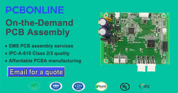
One-Stop PCB Services Including Design, Fabrication, Assembly, and Testing
Choosing the right PCB design tool is the start of your electronic engineering journey. Choosing the right PCB supplier is as important or even more important than it.
PCBONLINE is an advanced PCB manufacturer for automotive, defense, medical, industrial, computing, and consumer applications. It provides one-stop PCB services from A to Z, including prototyping, volume fabrication, assembly, and testing until you receive satisfactory products.
By working with PCBONLINE, you can make sure of the optimum PCB design and products for the following reasons:
- PCBONLINE provides free DFM, DFT, DFA, and DFX for PCB fabrication, PCB assembly, and box builds.
- When receiving your Gerber and BOM, the professionals from PCBONLINE deeply study your requirements and give a quote.
- PCBONLINE can take part in the R&D of your project and provide an optimal PCB design to reduce the fabrication cost without function sacrifice.
- PCBONLINE provides one-on-one engineering support throughout your project until the products reach your expectations.
When making sure of the PCB design and engineering, PCBONLINE's strong PCB and PCBA capabilities can meet the fabrication needs of your project:
|
Types of PCB
|
PCB layer quantity
|
Copper thickness
|
Minimum line space/width
|
|
FR4 PCB
|
1 to 64
|
0.5oz to 14oz
|
0.0635mm/0.0635mm
|
|
Aluminum PCB
|
1 to 4
|
1oz to 4oz
|
0.1mm/0.1mm
|
|
Copper-base PCB
|
1 to 8
|
1oz to 10oz
|
0.1mm/0.1mm
|
|
Ceramic PCB
|
1 to 4
|
5μm to 10oz
|
5-10μm: 0.05mm/0.05mm
Hoz: 0.075mm/0.075mm 1oz: 0.1mm/0.1mm 2oz: 0.127mm/0.127mm 3oz: 0.3mm/0.3mm 6oz: 0.5mm/0.5mm 9oz: 0.6mm/0.6mm |
|
High-frequency PCB
|
4 to 24
|
0.5oz and 1.0oz
|
0.0635mm/0.0635mm
|
|
Flexible PCB
|
1 to 10
|
25μm to 3oz
|
0.04064mm/0.04064mm
|
|
Rigid-flex PCB
|
2 to 24
|
1/3oz to 3oz
|
0.04064mm/0.04064mm
|
|
HDI PCB
|
4 to 64
|
100μm to 125μm
|
0.04064mm/0.04064mm
|
|
1
|
4μm to 25μm
|
0.15mm/0.15mm
|
If you have any plans of informing your concept or electronic design into reality, you can send your Gerber, request, or question to info@pcbonline.com.
Conclusion
This blog tells how to bake printed circuit boards and electronic components, including the baking temperatures and duration. If your PCBs or components need baking before the assembly, PCBONLINE is a reliable one-stop service option.


