Advantages of the PCB Manufacturer PCBONLINE
 MATERIALS
 Ceramic PCB fabrication at PCBONLINE uses 99.96% aluminum nitride or aluminum oxide and metal layers with low resistance and strong adhesion.
 EQUIPMENT
 PCBONLINE has equipment for laser depaneling for round ceramic PCBs and diamond-cut for rectangular ceramic PCBs.
 TEAM
TEAM The professionals from PCBONLINE apply DPC technology to realize 3-D circuit design. HTCC, DBC, LTCC, thick-film, thin-film, and AMB PCBs are also available.
 QUALITY
 PCBONLINE provides ceramic PCBs without an oxide layer that can be used for a long time in aggressive environments.
 CUSTOM
 The thickness of copper is arbitrarily customized from 1μm to 1mm at PCBONLINE. And its HDI capability can realize the small size, lightness, and thinness of the product.
 TRANSPORT
 PCBONLINE provides various ceramic PCB shipping methods, including air, sea, and rail shipping by DHL, FedEx, and UPS. You can choose your freight forwarder.
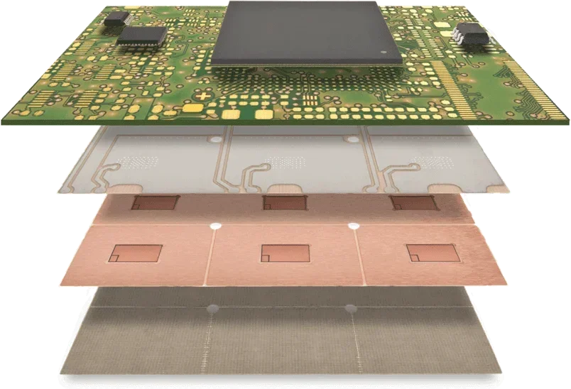
Ceramic PCB Manufacturing
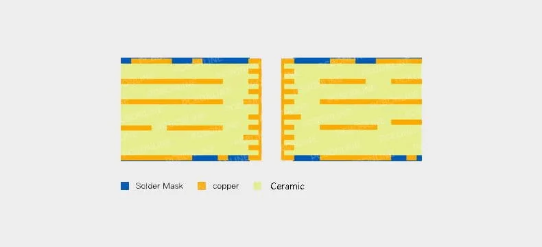
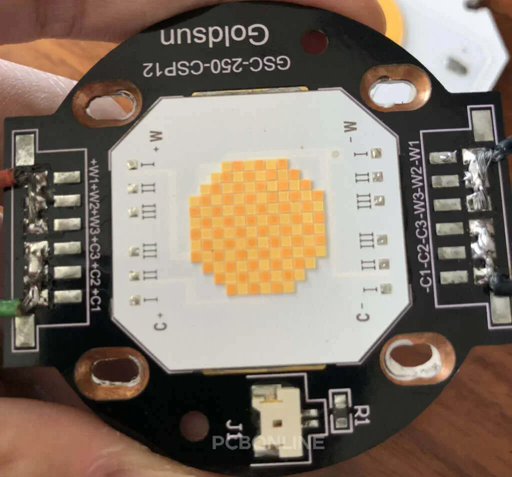
Ceramic PCBs have one ceramic substrate, and the copper layers are sputtered, plated, sintered, or brazed on the top and bottom sides of the ceramic substrate.
According to the different ceramic materials, there are AlN PCBs, alumina PCBs, SiC PCBs, Si₃N₄ PCBs, BeO PCBs, and hybrid ceramic PCBs.
According to the different ceramic PCB manufacturing processes, there are LTCC, HTCC, DPC, DBC, thick-film, thin-film, and AMB PCBs.
In ceramic PCB fabrication, PCBONLINE adopts two different lamination methods according to specific requirements.
Normal lamination: In the ceramic PCB lamination process under high-temperature and high-pressure conditions, two ceramic substrate layers are bonded by a dielectric layer (PP). The PP materials are mainly phenolic, epoxy resin, and special thermal conductive materials.Sintering lamination: In the PCB lamination process under high-temperature and high-pressure conditions, molecules of the two ceramic substrate layers' contact surfaces migrate, and the two layers integrate and form dense polycrystalline ceramics as a whole (relative density > 98%).
The normal lamination process's manufacturing cost is low, but it drastically reduces the overall thermal conductivity of the ceramic circuit board, and its bonding strength is not as good as sintering lamination.
If the PCB requires high thermal conductivity, we use the sintering lamination method. This technology bonds the copper and the ceramic material together with a strong bonding force and high reliability. Meanwhile, the characteristics of the ceramic substrate are not affected, especially the thermal conductivity and flatness.
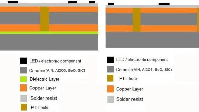
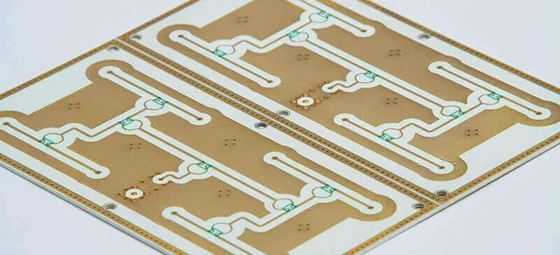
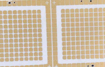
Direct Plating Copper (DPC) for Ceramic PCB Manufacturing
DPC is one of the ceramic circuit processing technologies at PCBONLINE. It developes from the thin-film PCB manufacturing process.
The DPC PCB process includes ceramic surface metalization, sputtering, copper plating, film exposure and development. Its ceramic PCB manufacturing flow is:
step 1. clean the ceramic substrate by pre-treatmentstep 2. sputter the ceramic substrate by vacuum coating to bond to the copper composite layerstep 3. use the photoresist coating of yellow light for exposure, development, etching, and film removal to complete the circuit productionstep 4. increase the copper thickness by electroplating/electroless platingstep 5. remove the photoresist, and the metalized circuit is done
Compared with the thick film and thin-film processing technologies, the DPC technology provides faster processing, a micron-rating fine process, and no ceramic type and thickness limit.
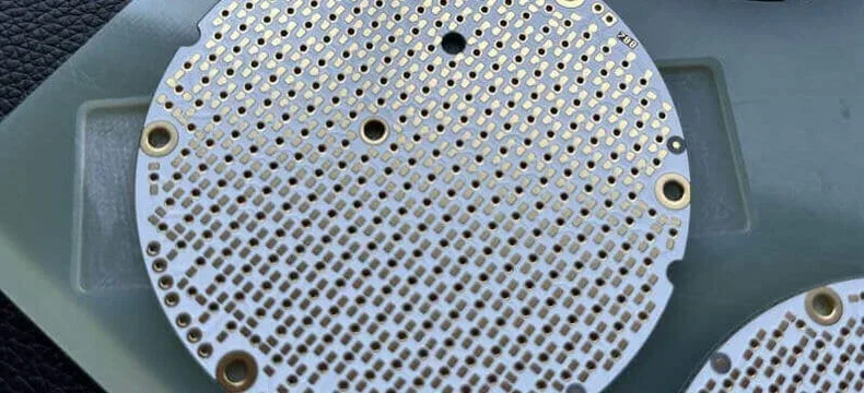
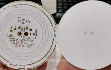
Ceramic PCB Depaneling at PCBONLINE
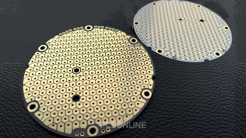
PCB depaneling is the step of removing single ceramic PCBs from the entire panel. At PCBONLINE, depaneling after the ceramic PCB fabrication or assembly can be laser-cut or diamond-cut. (V-cut and CNC can't depanel ceramic PCBs.)
Laser PCB depaneling for round ceramic PCB: To protect the circuit from high temperatures, at the laser head, nitrogen is used to lower the PCB temperatures. Then we clean and remove the carbon along with the depaneling round line.Diamond PCB depaneling: Similar to V-cut, the depaneling line of the ceramic PCB has to be straight. Ceramic PCBs are depaneled under room temperatures, so you don't need to worry about carbonization. In addition, PCBs can be panelized on the production panel.
PCBONLINE suggests designing the ceramic PCBs as rectangular or squire as possible. But round ceramic PCB manufacturing is okay for PCBONLINE. We provide professional engineering support to your project to penalize your ceramic PCBs and avoid carbonization.
Ceramic PCB Manufacturing Capabilities
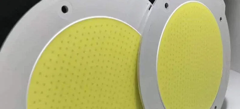
Applications of ceramic PCB:
high-power electronic modules, solar panel componentshigh-frequency switching power supplies, solid-state relayscommunication antennasautomotive sensors, refrigeration sheets, etc
GET A FREE QUOTE
PCB and PCBA Certifications


Contact Our Expert Team Now

Learn about our products


Get customized services

 Phone
Phone WhatsApp
 Email
Email
Offer Electronics Manufacturing All-in-One
PCBONLINE® is a registered trademark or service mark of pcb online limited or its affiliates.
Copyright © 2005-2025 Pcb Online Limited. All rights reserved


