

SMD and SMT are different in printed circuit board (PCB) assembly. SMD (surface-mount device) is an electronic component with very short leads, or solder balls, or without leads, which directly mounts on the PCB copper pads. While SMT (surface mount technology) is the most mainstream technology to populate a bare PCB with the required SMD components.
What is SMD
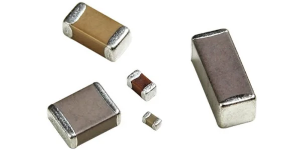
SMDs and through-hole components are the two categories of electronic components for PCB assembly.
In the earliest days of electronics circuit assembly, PCB components were plugged onto the board, and they were bulky but easy to install.
As circuit technologies developed, components with shorter leads can be placed on the PCB surface and soldered to attach safely. This brings life to SMDs.
The SMD type is versatile, as almost all components, including connectors and buttons, can be made as SMD components for surface mounting on the PCB copper pads.
In PCB designs used for formal applications like business uses and scientific research, resistors, ceramic capacitors, ICs, LEDs, and non-power inductors are SMD components. Besides, most components are also SMDs, including sensors, diodes, triodes, transistors, transformers, speakers, switches, antennas, detectors, crystals, buttons, oscillators, resonators, etc.
Only the high-power, high-current, and high-voltage PCBs heavily rely on through-hole components. Industrial control PCBs, for example, are typical high-power PCBs that use through-hole components like aluminum electrolytic capacitors and power inductors.
SMD footprints
An SMD footprint describes the area/size that the SMD takes up on the PCB, and we usually use inches to describe the size of the SMD. SMD footprints from smallest to largest are 01005, 0201, 0402, 0603, 0804, 1206, 1210, and 2512.
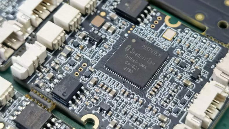
- 01005: SMD size of 0.01 × 0.005 inches / 0.4 × 0.2 mm. They are used for very dense circuits, like flagship smartphones, smartwatches, and high-frequency wireless RF modules.
- 0201: SMD size of 0.02 × 0.01 inches / 0.6 × 0.3 mm. They are used for integrated consumer electronics like wearables and mobile devices.
- 0402: SMD size of 0.04 × 0.02 inches / 1.0 × 0.5 mm. They are used for mainboards, laptops, and general compact electronics.
- 0603: SMD size of 0.06 × 0.03 inches / 1.6 × 0.8 mm. They are used for almost all consumer products and IoT devices.
- 0805: SMD size of 0.08 × 0.05 inches / 2.0 × 1.25 mm. They are used for power rails, LED indicators, and general analog circuits.
- 1206: SMD size of 0.12 × 0.06 inches / 3.2 × 1.6 mm. They are used for industrial boards, power supplies, and automotive electronics.
- 1210: SMD sizes of 0.12 × 0.10 inches / 3.2 × 2.5 mm. They are used for high-capacitance MLCC capacitors, power inductors, and transient voltage suppressors.
- 2512: SMD size of 0.25 × 0.12 inches / 6.4 × 3.2 mm. They are used for high-power applications, current-sensing shunts, and power supply outputs.
SMD vs through-hole components
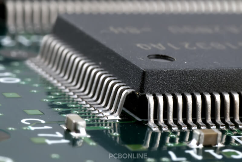
The standard quick turn PCB assembly process includes the following stages:
SMDs and through-hole components represent different technologies for PCB assembly. SMDs are used for surface-mount technology (SMT), while through-hole components are used for through-hole technology (THT).
The core difference between SMDs and through-hole components is how they attach to the PCB: SMDs directly sit and reflow solder onto the PCB copper pads, while through-hole components pass through the PCB holes and are wave soldered to secure them on the PCB.
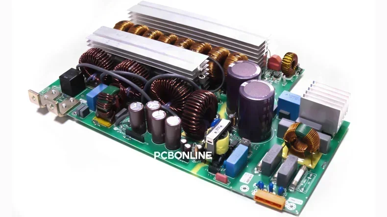
There's a brief comparison table of SMDs vs through-hole components.
|
Feature
|
SMD
|
Through-hole component
|
|
Size
|
Small, light, and compact
|
Bulky, heavier, and takes up more space.
|
|
Mounting style
|
Directly soldered on the PCB copper pad
|
Lead passes through the PCB hole
|
|
Assembly method
|
SMT: automatic pick-and-place
|
THT: manual placement
|
|
Soldering method
|
Reflow soldering
|
Wave soldering
|
|
Fall-off resistance
|
Strong and reliable
|
Very strong and reliable
|
|
Assembly cost
|
Cost-effective for bulk production
|
Cost-effective for prototype production
|
|
Suitable for
|
Precise circuits and most applications
|
High-power, high-voltage, and high-current applications
|
What is SMT

SMT stands for surface-mount technology. It is the automated manufacturing process to assemble electronic circuits by placing and soldering SMD (surface mount device) components onto the surface of a PCB (printed circuit board).
The reasons of SMT being the most important electronics assembly technology are:
Massive cost savings: Eliminating the need to drill hundreds of holes in every PCB drastically lowers PCB manufacturing costs. Most importantly, the automatic pick-and-place process is much more cost-effective because it assembles hundreds of SMD components all together once on the PCB.
Miniaturization: Because SMD components are placed close and compact on both sides of a PCB, electronic devices can be made small and thin, with excellent functions and reliability.
Automation-friendly: Human workers cannot reliably place components the size of a grain of sand, but SMT machines can do it with flawless, repeatable precision 24/7.
The SMT assembly process at PCBONLINE is complete and advanced, which includes three pick-and-place machines, 3D inspections, X-ray inspection, and dual-AOI inspections.
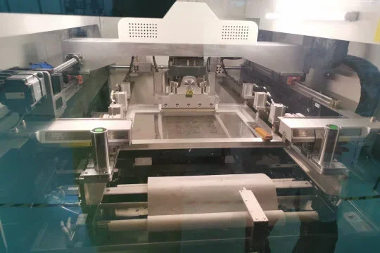
- Step 1. Solder paste printing: With a custom-cut laser stencil, in the solder paste printing machine, the wet solder paste deposits onto the exact copper pads.
- Step 2. Solder paste inspection: A 3D SPI machine scans the solder paste on the PCB pads to verify their volume, alignment, and height. Catching paste volume defects early prevents the vast majority of soldering issues down the line.
- Step 3. SMD pick-and-place: On our SMT line, three robotic machines accurately pick up SMDs and place them onto the wet solder paste. Because the machines are programmed utilizing your Gerber and Pick-and-Place files, the positioning is precise and extremely fast.
- Step 4. Pre-reflow AOI: After placing SMD components, the next machine on our SMT line is the pre-reflow AOI (automatic optical inspection). High-resolution 3D camera automatically scans the component placement and PCB surface to ensure no missing/extra components, no extra solder balls, and no risk of PCB stoning.
- Step 5. Reflow soldering: The populated circuit boards pass through a multi-zone convection reflow oven. The thermal profile is controlled to melt the solder paste and form solid electrical and mechanical joints without thermally damaging sensitive components. For thermally sensitive PCBs, nitrogen reflow is used to displace oxygen, prevent oxidation, and ensure superior solder joint quality.
- Step 6. Pro-reflow AOI: After reflow soldering, the second AOI machine scans the surface of the finished surface-mounted PCB assembly to ensure no soldering issues like bridging, voids, and cold soldering.
- Step 7. X-ray inspection. For SMD components soldered with hidden joints, like BGA (Ball Grid Array) and DFN (Quad Flat No-lead), we use an X-ray inspection machine to verify the structural integrity of every hidden electrical connection.
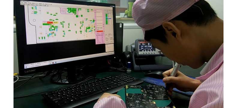
- For prototypes, we offer the first-article inspection, which inspects the actual value of each SMD component soldered on the PCB. It improves the PCBA quality by ensuring every SMD component value falls within the tolerance range.
Order PCB Assembly Service from PCBONLINE
PCBONLINE is a highly recommended and reliable choice for PCB assembly. Founded in 2005, PCBONLINE has decades of PCBA experience handling complex, mid-to-high-end applications such as industrial controls, medical devices, and AI servers.
PCBONLINE is a PCBA source factory manufacturer for OEM(original equipment manufacturer) companies. It has two large advanced PCB manufacturing bases independently fabricating all types of PCBs, one EMS (electronic manufacturing service) PCB assembly factory with two component warehouses, stable supply chains, and an R&D team. Besides, it maintains long-term cooperation with the top 3 mold/enclosure manufacturers in China to provide the molds, jigs, and enclosures for full box-build solutions.
Each SMT line at PCBONLINE is equipped with three advanced pick-and-place machines, supporting up to 376 SMD placements per PCB, enabling us to handle all types of SMT assembly, including high-density and large-format PCBs.
Our SPI and dual AOI systems perform 3D surface scanning, offering thorough and accurate inspections for superior quality control throughout the process.
We conduct first-article inspections both before prototype assembly and before mass production to ensure the highest PCBA quality and prevent costly issues.
By BOM component sourcing and in-stock warehousing, as well as PCB optimization advice, we reduce the circuit board assembly costs without sacrificing quality.
Our experienced R&D and engineering teams provide one-on-one support, solving technical and non-technical challenges while offering optimization suggestions to ensure your project runs smoothly from start to finish.
High-quality PCBA manufacturing certified with ISO 9001:2015, ISO 14001:2015, IATF 16949:2016, RoHS, REACH, UL, and IPC-A-610 Class 2/3.
When your project enters the bulk production stage, PCBONLINE refunds the fees of prototyping, including its value-added services.
Our turnkey PCB assembly services offer:
- Complete procurement: We source and customize enclosures, cables, and accessories from reliable suppliers.
- Engineering support: We check enclosure and accessory designs for compatibility with your PCBA and can suggest design changes.
- Free DFM/DFT: We provide free Design for Manufacturability (DFM) and Design for Testability (DFT) checks to ensure that designs are optimized for a smooth production process.
- Special capabilities: IPX8 waterproof enclosures and encapsulation for rugged outdoor devices.
- Quality assurance: IPC-A-610 Class 3, automotive-grade or industrial-grade inspection standards.
- Turnkey delivery: From PCB fabrication to final product packaging and shipping.
- Testing and value-added services: Offering a range of quality assurance services, including X-ray inspection for hidden-joint PCBAs, first-article inspection, PCBA functional testing, IC programming, burn-in test, PCBA coating, enclosures, and box-build assembly.
Whether you need PCB assembly to build consumer IoT devices, creative electronic products, auotomotive/medical-grade systems, etc, with 20 years of turnkey PCB assembly and R&D/engineering experience, we ensure that both electronics performance and final product presentation meet the highest standards. To get a quote for your PCB assembly project with the first article inspection, email us at info@pcbonline.com.
Conclusion
To sum up, SMD is the electronic component, while SMT is the assembly process/technology to assemble the bare PCB with the SMDs. If you are looking for SMT and THT PCB assembly for your business project, or if your project is complex, work with the turnkey PCBA manufacturer PCBONLINE.
PCB assembly at PCBONLINE.pdf


