
As artificial intelligence applications emerge more and more, the Internet of Things (IoT) electronics embrace higher and higher demands in the market. PCB assembly for IoT electronics is usually ordered by OEM terminal companies and business makers, which is turnkey, covering everything from PCB fabrication to box-build assembly.
Minimization and High-Density Trends for IoT PCB Assembly
IoT devices are getting progressively smaller, like smart rings, AI glasses, subcutaneous glucose monitors, and compact home security sensors. IoT electronic devices pack a massive amount of computing power into tiny spaces. Miniaturization in PCB assembly is the inevitable trend.
To achieve small footprints like 0201 and 01005, IoT PCB manufacturers like PCBONLINE rely on high-density interconnect (HDI) PCBs. HDI PCBs allow engineers to place more components in a smaller area with connections by laser-drilled microvias, blind vias, and buried vias. HDI technology reduces the overall size and weight of the final IoT product.
Flexible and rigid-flex PCBs are also used to create IoT electronic devices. Many IoT devices have unconventional shapes, as a standard rigid PCB does not fit inside a curved wearable device or a compact tracking tag. Flexible circuits solve this spatial problem. They can bend, twist, and fold to fit tight enclosures.
The PCB assembly line for IoT electronics must be able to handle tiny 0201 and 01005 surface-mount devices (SMDs). High-speed, high-accuracy pick-and-place machines are mandatory.
Power management is another major design factor. Many IoT devices operate on compact batteries. They need to run for months or even years without a charge. The PCB design must minimize power loss. PCB assembly for IoT devices must ensure solid, low-resistance solder joints to prevent phantom power drain.

Thermal management is also critical. Fine-pitch microchips generate concentrated heat so the PCB must dissipate heat quickly to protect sensitive components. So the FR4 PCB material used for IoT electronics has a high Tg with higher temperature resistance.
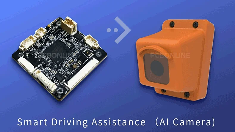
Furthermore, IoT devices rely heavily on wireless communication like Wi-Fi, Bluetooth, or LoRa. Dealing with the Radio Frequency (RF) section is tricky, as the antenna trace must have perfect electrical impedance. The turnkey PCB assembly manufacturer for PCBONLINE provides.
Market Growth of PCB Assembly for IoT Electronics
The global demand for IoT devices is continuously exploding, which drives the rapid growth of the PCB assembly market. According to recent industry reports, the global IoT market size is projected to reach over USD 1,055 billion in 2026. It is expected to grow at a compound annual growth rate of over 23% through 2034.

Consequently, the PCB assembly for the IoT electronics market is thriving alongside. The global PCBA market is estimated to reach around USD 108 billion in 2026. A massive portion of revenue comes directly from IoT and smart device manufacturing.
Several factors fuel the rapid market expansion of IoT electronics assembly. First is the global rollout of AI hardware and optical communication infrastructure. Stronger computing power and faster cellular networks allow IoT devices to transmit heavy data instantly, sparking new applications in AI servers, autonomous driving, remote healthcare, and smart cities. All these applications require high-performance PCB assemblies.
Second, the smart home sector is booming worldwide, including connected thermostats, security cameras, and smart appliances. AI integration makes these devices smarter and more intuitive. Industry data shows that AI-enabled devices could account for nearly 40% of the smart home market by 2026.
Third, industrial IoT (IIoT) is transforming traditional manufacturing. Wireless sensors monitor equipment health and optimize production lines and vehicles. These industrial sensors must survive harsh, dirty factory environments and require highly reliable PCBs.
Finally, medical IoT is seeing unprecedented growth, like wearable medical devices that track patient health remotely and transmit vital data to doctors. Medical PCBs demand strict quality certifications like ISO 13485. Medical device OEMs outsource electronics production to turnkey electronics manufacturing services (EMS) providers like PCBONLINE, allowing the OEMs to focus purely on software development and product marketing.
PCB Assembly Process for IT Electronics
Turnkey PCB assembly for IoT electronics covers every manufacturing step, which is ideal for hardware OEMs. It saves precious time, reduces global shipping costs, and ensures quality control.

Let us walk through the PCB assembly process from the bare PCB to the final packaged box-build.
1. PCB fabrication
Based on the customer's Gerber files, the factory fabricates the PCB by pressing together multiple layers of fiberglass and copper. Many wireless IoT devices require high-frequency materials like Rogers laminates to prevent wireless signal loss.

We drill tiny microvias using highly precise lasers by plating the holes with copper to connect the internal layers electrically. Finally, we apply a protective solder mask and a surface finish. Electroless Nickel Immersion Gold (ENIG) is a popular choice for IoT PCBs.
2. Solder paste printing and inspection
Once the bare PCBs are ready, the PCB assembly can begin. The first step is applying solder paste. A custom-cut stainless steel stencil is placed over the PCB. A mechanical squeegee pushes solder paste through the holes in the stencil and lands on the copper pads where components will sit.
After printing, a 3D solder paste inspection machine thoroughly scans the PCB, checking the volume, alignment, and shape of the wet paste.
3. SMT component placement
Next is Surface Mount Technology (SMT) assembly. The PCB enters two robotic pick-and-place machines. One picks up tiny resistors, capacitors, and inductors from component reels. The other picks up microchips, connectors, and sensors onto the wet solder paste.
4. Pre-reflow AOI and reflow soldering
The PCB is scanned by an automatic optical inspection (AOI) machine before traveling on a conveyor belt into a reflow oven. The oven has multiple controlled heating zones to slowly raise the temperature. The flux in the paste activates and cleans the metal surfaces. Then, the temperature peaks, melting the solder alloy. The PCB cools down slowly, forming strong electrical and mechanical joints. Nitrogen reflow is often used for IoT PCB assembly to reduce oxidation.
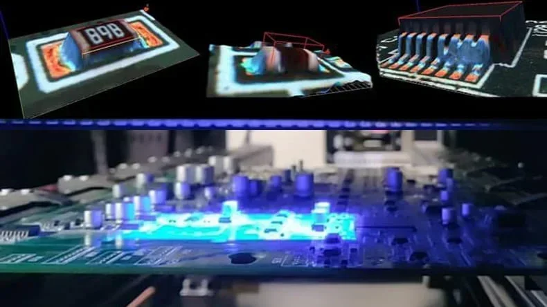
5. Post-reflow AOI and X-ray inspection
After soldering, the PCB assembly undergoes another AOI. High-definition cameras scan the assembly from multiple angles. The software looks for missing parts, skewed chips, or accidental solder bridges.
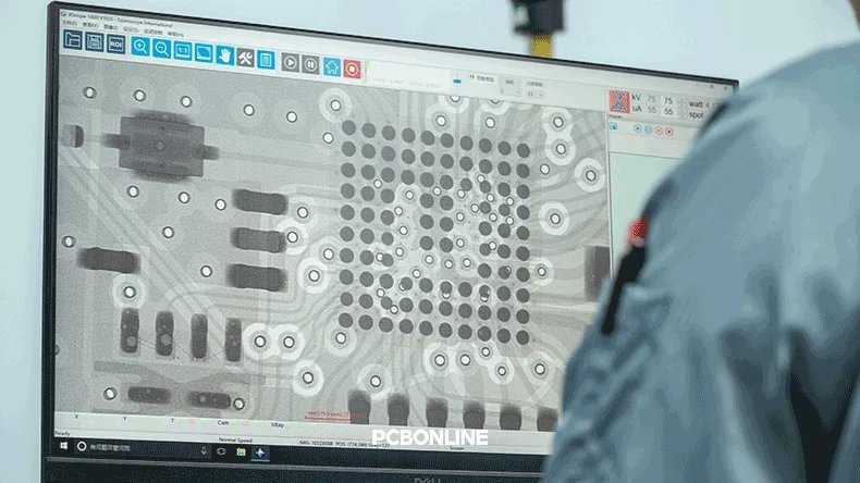
IoT PCBs frequently use chips like Ball Grid Arrays (BGAs). BGA chips have their solder joints hidden completely underneath the package. Therefore, an X-ray inspection machine is used. The X-ray penetrates through the chip. It ensures every hidden connection is solid and free of internal air voids.
6. THT component placement and wave soldering
Some IoT devices also use Through-Hole Technology (THT) components, including bulky power connectors, relays, or large capacitors. THT components have long metal leads that go straight through drilled holes in the PCB. Technicians place them manually, or we can also use an automated insertion machine.
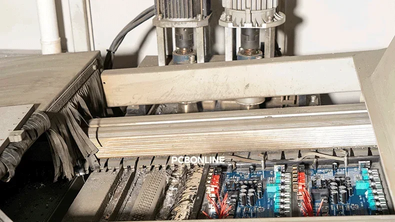
Then, the bottom of the PCB assembly passes directly over a flowing wave of liquid solder. The molten metal flows up into the holes and around the leads. It bonds the larger components securely to the circuit board.
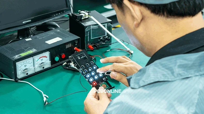
6. Firmware flashing and functional testing
Firmware flashing means loading the software onto the microcontrollers. This process is also called IC programming or flashing.
Next comes functional testing. The PCBA is powered on for the first time, and custom test rigs simulate real-world conditions by sending digital signals to the PCB assembly and measuring the physical output. Does the Wi-Fi module transmit data correctly? Does the temperature sensor read accurately? Do the status LEDs turn on? If the PCBA passes all these functional tests, it is verified as working hardware.
7. Conformal coating and potting
Many IoT devices operate outdoors or in harsh industrial environments with rain, high humidity, dust, and extreme temperature swings. To protect the sensitive electronics, a conformal coating is applied. This is a thin, invisible layer of chemical polymer, which seals the PCB assembly against moisture and chemical corrosion.
![]()
For extreme environments, some IoT PCB assemblies undergo full potting by encasing the entire PCBA in a solid block of silicone or epoxy resin. Agricultural soil sensors, automotive GPS trackers, and underwater monitors nay need to achieve high waterproof IP ratings.
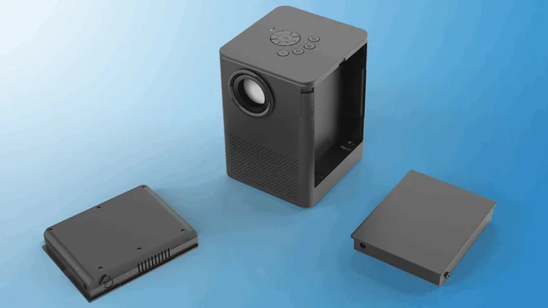
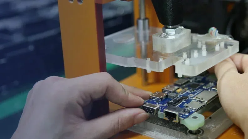
8. Final box-build assembly
The PCB assembly needs an outer enclosure. Box-build assembly involves putting the PCBA inside its custom plastic or metal casing and installing the harness cables, support standoffs, LCD screens, physical buttons, and rechargeable batteries. They secure the enclosure with screws or ultrasonic welding.
Finally, the fully assembled IoT device undergoes one last quality check. The finished IoT product is then packaged directly into its retail box. It is labeled, boxed up, and shipped directly to the OEM or drop-shipped.
Order OEM IoT PCB Assembly Service from PCBONLINE
PCBONLINE is a reliable choice for turnkey PCB assembly for IoT electronics. Founded in 2005, PCBONLINE has decades of experience handling complex, mid-to-high-end applications such as industrial controls, medical devices, and AI servers.
PCBONLINE is an OEM PCBA source factory manufacturer. It has two large advanced PCB manufacturing bases independently fabricating all types of PCBs, one EMS (electronic manufacturing service) PCB assembly factory with two component warehouses, stable supply chains, and an R&D team. Besides, it keeps long-term cooperation with the top 3 mold/enclosure manufacturers in China to provide the molds, jigs, and enclosures for full box-build solutions.
Each SMT line at PCBONLINE is equipped with three advanced pick-and-place machines, supporting up to 376 SMD placements per PCB, enabling us to handle all types of SMT assembly, including high-density and large-format PCBs.
Our SPI and dual AOI systems perform 3D surface scanning, offering thorough and accurate inspections for superior quality control throughout the process.
We conduct first-article inspections both before prototype assembly and before mass production to ensure the highest PCBA quality and prevent costly issues.
By BOM component sourcing and in-stock warehousing, as well as PCB optimization advice, we reduce the circuit board assembly costs without quality sacrifice.
Our experienced R&D and engineering teams provide one-on-one support, solving technical and non-technical challenges while offering optimization suggestions to ensure your project runs smoothly from start to finish.
High-quality PCBA manufacturing certified with ISO 9001:2015, ISO 14001:2015, IATF 16949:2016, RoHS, REACH, UL, and IPC-A-610 Class 2/3.
When your project enters the bulky production stage, PCBONLINE refunds the fees of prototyping, including its value-added services.
Whether you need PCB assembly to build consumer IoT devices, creative electronic products, automotive/medical-grade systems, etc, with 20 years of PCBA manufacturing and box build experience, we ensure that both electronics performance and final IoT product presentation meet the highest standards. To get a quote for your IoT PCB assembly project, email us at info@pcbonline.com.
Conclusion
IoT PCB assembly is turnkey, including PCB fabrication, PCB assembly, testing, and box-build assembly. If you look for PCB assembly for IoT electronics, work with the turnkey PCBA manufacturer PCBONLINE.
PCB assembly at PCBONLINE.pdf


