
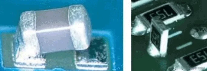
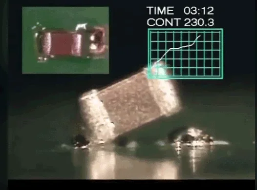
The tombstone effect in PCB, also known as the Manhattan effect or PCB tombstone, is a Surface Mount Technology (SMT) assembly defect, where a small chip-type passive component (such as 0402/0603 resistors and capacitors) stands vertically on one of its terminations after reflow soldering.
No worries about tombstoning in PCB by partnering with the turnkey PCB assembly manufacturer PCBONLINE! At PCBONLINE, we have systematic approaches and rich design for manufacturing (DFM) experience to prevent tombstoning PCB from occurring.
Causes of Tombstoning in SMT PCB Soldering
First, let's understand why PCB tombstoning occurs before we find the cures to prevent this PCB soldering defect.
Tombstoning occurs when uneven surface tension pulls one end of the chip component to lift during reflow soldering. It leads to an open circuit or weak solder joint.
If the tombstone phenomenon occurs, the open circuit fails the PCBA. Even a partial tombstone can increase contact resistance after thermal cycling, and can develop into a complete open circuit under vibrations.
The root causes of the PCB tombstoning are from several aspects:
Uneven heating during reflow soldering
If one pad heats up faster than the other, the solder paste on that side melts first, creating a stronger wetting force that pulls the component upward.
PCBONLINE has rich experience in reflow oven temperature control. We will use slow and controlled preheating (typically 150°C ±10°C for 60-90 seconds) helps synchronize solder melting and prevents tombstoning.
Poor solder paste printing
Inconsistent solder paste deposition (e.g., one pad has more paste than the other) leads to uneven wetting forces.
Solder paste thickness plays a crucial role—thinner stencils (e.g., 0.1mm for 0603 components) reduce tombstoning risk.
Our experienced engineers will design the SMT stencil to let the solder paste go through the stencil holes accurately on the PCB pads.
Incorrect pad design
Asymmetric pad sizes or excessive pad extensions can cause uneven thermal distribution. If the two pads are designed with different sizes, PCB tombstoning occurs.
PCBONLINE, according to IPC-7351 standards, will recommend symmetrical pad designs to ensure balanced solder wetting forces.
Besides, if you place the chip component with the orientation parallel with the reflow oven's conveyor, the reflow wind may blow its one terminal to lift, causing tombstoning. In such a case, PCBONLINE's engineers will suggest that you change the component's orientation to be vertical with the reflow oven's conveyor.
Component misalignment during placement
If a component' terminal does not cover more than 50% of the PCB pad, it does not properly contact the solder paste, leading to tombstoning. When our professionals at PCBONLINE notice this in our free DFM for your project, we will advise you to reduce the space between the two pads.
Poor solder paste quality or oxidation
Expired or improperly stored solder paste can lead to poor wetting and increase tombstoning risk.
Oxidized component terminations may prevent proper solder adhesion, causing one side to lift.
Besides, if you choose nitrogen reflow soldering to prevent the risk of PCBA oxidation, nitrogen tends to increase the PCB tombstone risk. However, PCBONLINE will handle nitrogen reflow with professionalism to prevent it.
How PCBONLINE Prevents Tombstoning in SMT Assembly
As a PCBA manufacturer for mid and high-end applications, PCBONLINE will never let any tombstoning happen! Though tombstoning PCB can be fixed, the PCBA quality won't be as good as the smoothly manufactured ones. For high-end applications requiring IPC-A-610 Class 3 level reliability, such as automotive, medical, and aerospace electronics, PCBONLINE pays every attention to prevent PCB tombstoning and doesn't allow it on any boards.
PCBONLINE prevents PCB tombstoning through our advanced solder paste management, SMT stencil design, DFM, and comprehensive inspection processes. Our approach has successfully eliminated tombstoning defects in our high-volume PCB assembly production.
Here's how we ensure zero tombstoning in our SMT assembly:
Professional DFM
For every PCB, PCBA, and box-build project, no matter what quantity you want, PCBONLINE will design your PCB Gerber files, BOM, enclosures, and test files carefully and suggest any improvements.
We ensure no pad design defects, component placement errors, etc, to prevent PCB tombstoning risks.
Besides, we design the SMT stencil, PCBA test fixtures, reflow profile, and PCBA manufacturing process to ensure proper solder paste printing, pick-and-place, and reflow soldering.
We will also solve any technical and non-technical issues throughout your project.
Precision solder paste management
Solder paste quality directly impacts solder joint reliability. PCBONLINE uses a smart solder paste cabinet for solder paste management, and we follow best-in-class solder paste handling practices:
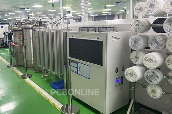
- Controlled storage & handling: Solder paste is stored at 0°C–12°C to maintain flux activity and prevent oxidation. Before use, it is thawed for 8 hours at room temperature and hand-mixed (not machine-mixed) to avoid viscosity changes.
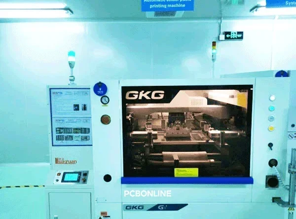
- Optimal printing conditions: Our SMT stencil printers maintain a stable environment (22°C–26°C, 45%±5% RH) to prevent paste drying. We use laser-cut stencils with precise thickness control (e.g., 0.1mm–0.15mm for fine-pitch components).
Optimized stencil design for balanced solder deposition
PCBONLINE's stencil design follows IPC-7525A standards to ensure uniform solder paste release.
Aperture size & shape: For 0402/0603 components, we use 1:1 pad-to-aperture ratios to prevent excessive solder volume. Trapezoidal apertures improve paste release and reduce bridging risks.
Step stencils for mixed components: When assembling mixed-size components, we use step stencils (locally thicker areas for large components, thinner for small ones) to balance solder deposition.
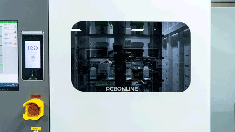
Dual AOI inspection (pre- & post-reflow)
PCBONLINE employs Automated Optical Inspection (AOI) before and after reflow to detect potential tombstoning risks.
Pre-reflow AOI: Checks solder paste deposition accuracy and component placement alignment. Detects missing paste, misaligned components, or skewed placements that could lead to tombstoning.
Post-reflow AOI: Verifies solder joint integrity and component positioning. Identifies tombstoned components, solder bridges, or insufficient wetting.
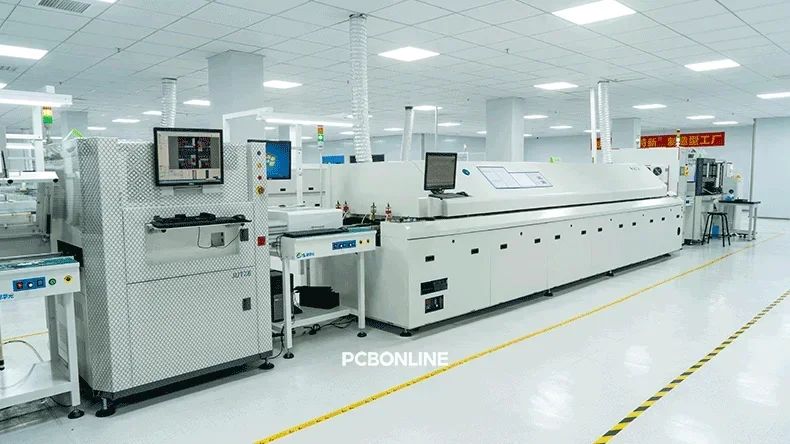
Optimized reflow profile for balanced melting
PCBONLINE's reflow ovens are calibrated to prevent rapid temperature spikes.
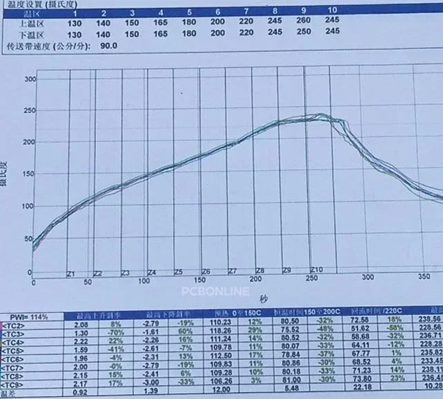
Gradual Preheating (1.5°C–2°C/s) ensures uniform pad heating.
Controlled peak temperature (230°C–250°C for lead-free solder) prevents component warping.
Nitrogen-assisted reflow (optional) reduces oxidation and improves wetting.
Strict component & PCB quality control
We verify the solderability of all incoming components.
For PCB pad symmetry, we check and ensure balanced thermal mass for even heating.
Why Choose PCBONLINE for PCB Assembly Services?
Tombstoning is a preventable defect when proper process controls, material management, and inspection techniques are applied. PCBONLINE promises that no boards manufactured by us have the tombstoning defect.
Founded in 1999, PCBONLINE is a trusted one-stop PCB assembly service provider for PCB manufacturing, PCB assembly, value-added, and box-build assembly.

PCBONLINE has two large advanced PCB manufacturing bases, one turnkey PCB box build assembly factory, stable material supply chains, and a dedicated R&D and engineering team. We also maintain long-term partnerships with top fixture and enclosure manufacturers in China.
Provides one-on-one free and professional DFM for PCB, PCBA, and box builds before and during prototyping/sampling, to ensure the manufacturability and project success.
Precision solder paste handling to maintain optimal viscosity and wetting properties, and IPC-compliant stencil designs for balanced solder deposition.
Dual AOI inspection to catch defects before and after reflow, and optimized reflow profiles for uniform solder melting.
PCBONLINE manufactures, assembles, and tests from PCBs and PCBAs to box builds as a source factory manufacturer under one roof, from prototypes to bulky production, saving costs and time for you.
High-quality PCBA manufacturing certified with ISO 9001:2015, ISO 14001:2015, IATF 16949:2016, RoHS, REACH, UL, and IPC-A-610 Class 2/3.
PCBONLINE provides comprehensive PCBA value-added services such as PCBA functional testing, conformal coating, IC programming, burn-in, enclosures, box-build assembly, application test, labelling, packaging, and shipping.
PCBONLINE delivers high-reliability PCBA assemblies with zero tombstoning defects, making us a trusted partner for automotive, medical, and aerospace electronics. To get a quote for PCB assembly services, email us at info@pcbonline.com.
Conclusion
Tombstoning is caused by an imbalance in solder wetting forces between the two terminations of a chip component. To ensure the success of your PCB assembly projects, partner with the turnkey PCBA manufacturer PCBONLINE.
PCB assembly at PCBONLINE.pdf


