
We posted all the rigid PCB capabilities, including the diagrams, last week. On this blog page, you can check out the rigid-flex PCB capabilities at PCBONLINE.
Introduction of Rigid-flex PCBs
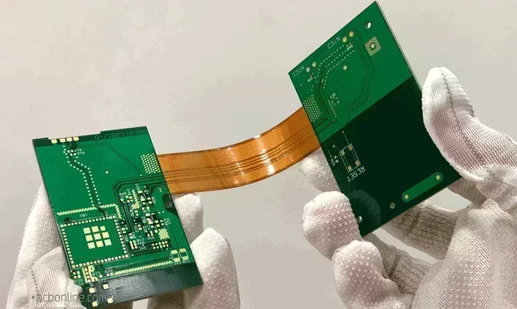
Rigid-flex PCBs are advanced printed circuit boards/printed wiring boards. Their inner laminate materials are PI (polyimide) and rolled annealed copper. The outer layers are FR4 PCB, and the non-wanted areas are laser cut.
Rigid-flex PCBs integrate the advantages of both rigid and flexible PCBs and can be made high-density interconnected (HDI). You can integrate your project design into a rigid-flex PCB for flexibility, minimum space, and light weight. Rigid-flex PCBs and PCBAs (printed circuit board assemblies) are installed in the corners and folds of notebooks, smartphones, automotive ABS detectors, wearable devices, tomographs, etc.
Rigid-flex PCB Manufacturing Capabilities
Now, let's see the capabilities of rigid-flex PCBs at PCBONLINE!
|
Rigid-flex PCB Specs
|
Rigid-flex PCB capabilities at PCBONLINE
|
|
|
Rigid-flex PCB layer count
|
2-64L
|
|
|
Flex Layer Count
|
11-20L (18L)
|
|
|
Flex laye on outer or Middle Layer
|
Middle
|
|
|
Finished board thickness
|
0.2-4.0mm
|
|
|
Tolerance of board thickness
|
>1.0mm, ±10%
≤1.0mm, ±0.1mm |
|
|
Min. flex layer width
|
2.5mm
|
|
|
Min. flex layer width between rigid layers
|
3mm
2mm (limit) |
|
|
Max. panel size
|
406x736mm
|
|
|
Min. panel size
|
10x15mm
|
|
|
Materials
|
Adhesive flex core
|
SF305: PI=0.5mil, 1mil, 2mil; Cu=0.33oz, 0.5OZ, 1OZ;
R-F777 PI=1mil, 2mil, 3mil, 4mil ,Cu =0.5oz, 1oz |
|
Adhesiveless core
|
Panasonic RF-775 (ED): PI=1mil, 2mil, 3mil; Cu=0.5OZ, 1OZ, 2oz
|
|
|
DuPont AP: PI=1mil, 2mil, 3mil; Cu=0.5 OZ, 1OZ
|
||
|
Thinflex W: PI=1mil, 2mill; Cu=0.5 OZ, 1OZ
|
||
|
at least 15/15mil
|
Shengyi SF305C series: 0515, 0525, 1025, 1035, 2030
|
|
|
TaiFlex FHK series: 0515, 0525, 1025, 1035, 2025
DuPont FR series: 0513 (FR7001), 1025 (FR0110) |
||
|
Thermosetting adhesive
|
TaiFlex series: AD=10um, 25um, 40um;
|
|
|
SF315B: AD=25um, 40um
|
||
|
PI stiffener
|
TaiFlex MHKseries: PI=3mil, 5mil; 7mil, 9mil;
|
|
|
3M tape
|
9460, 9077, 9458, 6677, 5907, 4920, 467MP
|
|
|
Low-flow prepreg (PP)
|
VT-47N; VT-901LF; EM-37B
|
|
|
Normal FR4
|
IT-180A; S1141, S1000-2; TU-768 (TU-752)
|
|
|
Special FR4
|
Arlon: 85N; Rogers: RO4350B series; Ventec: VT-901; M6 series: R-5775; TUC: TU-872SLK, TU-862HF
|
|
|
Impedance tolerance
|
Single-ended: ±3Ω (≤50Ω), ±8% (>50Ω)
Differential pair: ±4Ω (≤50Ω), ±8% (>50Ω) |
|
|
HDI type
|
3+n+3 (n buried hole≤0.4mm)
|
|
|
Min. Twist & Warp
|
0.75% (symmetrical);
1.5% (asymmetrical) |
|
|
Adhesive dispense width
|
1.5±0.5mm (slot width≥5mm))
|
|
|
Min. distance between R-F connect area to conductors
|
0.3mm (Half depth slot process)
0.5mm normal |
|
|
Min. width of resin flow out in R-F connect area
|
0.5mm
1.0mm normal |
|
|
Min. distance between E-test pads
|
3mil
4mil normal |
|
|
Min. inner layer line width/space before compensation
|
Finished copper thickness18um
|
3.5mil (partial3.2mil)/3mil (partial3mil)
|
|
Finished copper thickness 35um
|
3.5mil (partial3.2mil)/3.5mil (partial3mil)
|
|
|
Finished copper thickness 70um
|
5.5mil (partial5mil)/4.5mil (partial4.2mil)
|
|
|
Inner layer grid
|
Finished copper thickness 18um
|
5/5mil (after compensation)
|
|
Finished copper thickness 35um
|
6.5/5mil (after compensation)
|
|
|
Finished copper thickness 70um
|
10/8mil (after compensation)
|
|
|
Min. Inner layer annual ring width (IPCIII, before compensation)
|
4mil (≤6L), 8mil (7-11L), 12mil (≥12L)
|
|
|
Min. annual ring single side (laser hole, before compensation)
|
3mil (partial 2.5mil)
4mil (partial 3.5mil) |
|
|
Min. inner layer isolation strip width
|
8 mil
10mil normal |
|
|
Min. inner layer isolation annual ring width
|
5mil (≤6L), 6mil (7-11L), 10mil (≥12L)
|
|
|
Max. inner layer finished copper thickness
|
3oz
|
|
|
Min. distance between inner layer conductor and outline
|
8 mil
10mil |
|
|
Min. external layer line width/space before compensation (Rigid on top/bottom)
|
Finished copper thickness, before compensation
|
3.2mil (partial3.0mil)/3.0mil (partial3.0mil)
|
|
Finished copper thickness 35um, before compensation
|
3.5mil (partial3.2mil)/3.5mil (partial3.0mil)
|
|
|
Finished copper thickness 70um, before compensation
|
5.5mil (parital5.0mil)/5mil (partial4.5mil)
|
|
|
Min. external layer line width/space before compensation (Flex on top/bottom)
|
Finished copper thickness, before compensation
|
5.0mil (partial4.5mil)/4.5mil (4.2mil)
|
|
Finished copper thickness 35um, before compensation
|
5.5mil (partial5.0mil)/5.0mil (partial4.5mil)
|
|
|
Finished copper thickness 70um, before compensation
|
7.0mil (partial6.5mil)/ 6.0mil (partial5.5mil)
|
|
|
Min. annual ring for PTH in external layer (class II)
|
Finished copper thickness, before compensation
|
4mil
|
|
Finished copper thickness 35um, before compensation
|
5mil
|
|
|
Finished copper thickness 70um, before compensation
|
8mil
|
|
|
Min. annual ring for PTH in external layer (class III)
|
Finished copper thickness, before compensation
|
5mil
|
|
Finished copper thickness 35um, before compensation
|
6mil
|
|
|
Finished copper thickness 70um, before compensation
|
9mil
|
|
|
Min. gap between line and line on copper filling layer (before compensation)
|
5/6mil (partial4/5mil)
|
|
|
Min. gaps between pad to line and pad to pad on copper filling layer (before compensation)
|
5/5.5mil (partial4/4.5mil)
|
|
|
Min. gap between lines on resin filling layer (before compensation)
|
5/6mil (partial4/5mil)
|
|
|
Min. gaps between pad to line and pad to pad on resin filling layer (before compensation)
|
5/5.5mil (partial4/4.5mil)
|
|
|
Min. BGA pad size
|
10mil (electrical Ni/Au7mil)
12mil (Electrical Ni/Au8mil) normal |
|
|
Max. dry film tenting hole
|
6.5mm
4.5mm normal |
|
|
Min. distance between NPTH edge to external conductor before compensation
|
6mil
|
|
|
Max. external finished copper thickness
|
5 oz
4.5mm normal |
|
|
Min. distance between external conductor and outline
|
8mil
4.5mm normal |
|
|
Min. external PTH annual ring single side, before compensation
|
<35um finished copper thickness
|
4mil (<2mm); 6mil (2-4.5mm); 10mil (4.6-6.5mm)
|
|
35-70um finished copper thickness
|
5mil (<2mm); 8mil (2-4.5mm); 14mil (4.6-6.5mm)
|
|
|
>70um finished copper thickness
|
7mil (<2mm); 12mil (2-4.5mm); 18mil (4.6-6.5mm)
|
|
|
Drilling
|
Min. mechanical drill size
|
0.15mm (≤1.6mm)
0.2mm (≤2.5mm) |
|
Min. half-hole (pth) size
|
0.3mm
|
|
|
Laser blind via size
|
4mil-6mil (advance6mil)
|
|
|
Max. buried hole size
|
0.4mm
|
|
|
Max. drill hole size
|
6.3mm
|
|
|
Max. A/R for through hole
|
12:1
|
|
|
Max. A/R for laser blind hole
|
0.8:1
|
|
|
Min. gap between hole wall and conductor before compensation
|
5mil (≤6L), 6mil (7-11L), 10mil (≥12L) (after compensation)
|
|
|
Min. space between laser holes and conductor
|
6mil
|
|
|
Min. tolerance of NPTH
|
±2mil (limited+0, -2mil or +2mil, -0)
|
|
|
Slot drill bit diameter
|
0.40-1.60mm (board thickness≤2.50mm)
|
|
|
Tolerance of countersink
|
±0.15mm
|
|
|
Countersink hole size tolerance
|
±0.15mm
|
|
|
Min. distance between PTH hole wall and rigid-flex connect area
|
0.5mm (after compensation)
|
|
|
Min. distance between PTH holes
|
10mil (after compensation)
12mil normal (after compensation) |
|
|
Solder mask
|
Min. solder mask bridge (copper ≤1oz)
|
4mil (Green, Red, Blue), 5mil (Black), 8.0mil (on big copper area)
|
|
Min. solder mask bridge (copper 2-4oz)
|
6mil,
8mil (on big copper area) |
|
|
Min. solder mask opening larger than pad single side
|
2.5mil (partial 2mil)
|
|
|
Min. solder mask opening lsrger than NPTH hole signle side
|
4mil
|
|
|
Min. width of soldermask cover line (singleside)
|
2.5mil (partial1.5mil)
|
|
|
Max. finished hole size for via filled with Soldermask both side tenting
|
0.9mm
|
|
|
Max. solder mask plugging via in pad with both sides opening
|
0.55mm
|
|
|
Solder mask color
|
Green/matte green/Black/Blue/Red/White
|
|
|
Silk screen color
|
white/yellow/black
|
|
|
Carbon ink
|
Carbon thickness
|
NA
|
|
Min. gap between carbon pads
|
15mil
|
|
|
Min. gap between carbon and pads
|
10mil
|
|
|
Carbon pad larger than covering pad single side
|
4mil
|
|
|
Peelable mask
|
thickness
|
0.2-0.8mm
0.2-0.5mm normal |
|
Outline
|
Min. space between the central line of non-copper-exposed V-cut to internal/external circuits (H means board thickness)
|
H≤40mil: 12mil (20°mean V-cut angle),
13mil (30°), 14.6mil (45°) |
|
40
|
||
|
63
|
||
|
94.5
|
||
|
V-cut offset tolerance
|
±4mil
|
|
|
V-cut board thickness
|
0.4-3.2mm
≤0.6mm one side V-cut |
|
|
Tolerance of V-cut angle
|
±5°
|
|
|
V-cut angle
|
20°, 30°, 45°
|
|
|
Min. space for jump V-cut (0.8 |
8.5mm
|
|
|
Min. space for jump V-cut (1.6 |
11mm
|
|
|
Min. space for jump V-cut (2.4 |
18mm
|
|
|
Gold finger bevelling angle
|
20°, 30°, 45°, 60°
|
|
|
Gold finger bevelling tolerance
|
±5°
|
|
|
Gold finger bevelling remained thickness tolerance
|
±5mil
|
|
|
Min. distance between gold finger and tab
|
7mm
|
|
|
Min. gap between the side of gold finger and the outline edge line
|
8mil
|
|
|
Min. internal radius
|
0.3mm
|
|
|
Depth tolerance of depth-control groove milling
|
±0.10mm
|
|
|
Outline tolerance
|
±0.1mm
|
|
|
Rout slot tolerance (NPTH)
|
±0.10mm
|
|
|
Rout slot tolerance (PTH)
|
±0.13mm
|
|
|
Drill slot tolerance (NPTH length/width≥2)
|
±0.05mm
|
|
|
Drill slot tolerance (PTH length/width≥2)
|
±0.075mm
|
|
|
Drill slot tolerance (NPTH length/width<2)
|
±0.075mm
|
|
|
Drill slot tolerance (PTH length/width<2)
|
±0.1mm
|
|
|
The tolerance between Fiducial mark pad to Fiducial mark pad
|
≤300mm ±4mil
300-400mm ±5mil 400-500mm ±6mil >500mm ±7mil |
|
|
IPC Class 3
|
Yes
|
|
|
Certification
|
ISO 9001
|
Yes
|
|
ISO 14001
|
Yes
|
|
|
TS16949
|
NA
|
|
|
ISO13485
|
NA
|
|
|
TL9000
|
NA
|
|
|
AS9100
|
NA
|
|
|
OHSAS18001
|
On planning
|
|
|
QC080000
|
NA
|
|
|
SA8000
|
On planning
|
|
|
UL number
|
Yes
|
|
|
UL number (Canada)
|
|
|
|
Others Certificate
|
NA
|
|
One-Stop Rigid-flex PCB Manufacturer PCBONLINE
You've checked all the details of rigid-flex PCB manufacturing capabilities at the one-stop PCB/PCBA manufacturer PCBONLINE. Its rigid-flex PCB capabilities and certifications match the requirements for middle and high-end applications used in automotive, computers, commercial, and communication industries.

PCBONLINE offers one-on-one engineering support and can reduce your rigid-flex electronics project through PCB design optimization and choosing alternative components.
Being a source factory manufacturer with two larger advanced PCB manufacturing bases and one PCB assembly factory, PCBONLINE provides cost-effective rigid-flex PCB manufacturing and assembly. Don't hesitate to email PCBONLINE at info@pcbonline.com to turn your ideas into real boards and devices.
PCB fabrication at PCBONLINE.pdf


