
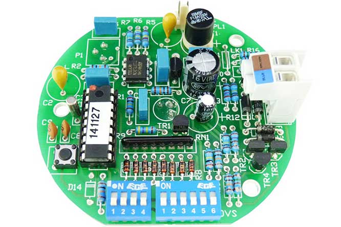
PCBONLINE is a one-stop advanced PCB manufacturers for middle and high-end applications. As our PCB fabrication page can't display all the PCB capabilities, we share all of our PCB manufacturing capabilities for rigid PCBs, flexible PCBs, and rigid-flex PCBs in the blogs.
This page shows the rigid PCB capabilities, including FR4 PCBs, metal-core PCBs, PTFE/high-frequency PCBs, HDI PCBs, and special material PCBs.
If you find that PCBONLINE's rigid PCB capabilities match your project requirements, please do not hesitate to contact us via the online chat window.
You can see PCBONLINE's rigid PCB capabilities below. For you to easily understand the PCB manufacturing items and processes in the table, we also insert diagrams.
|
Items or processes
|
PCB Capabilities at PCBONLINE
|
Diagram
|
|
|
PCB layer quantity
|
1-80L
|
|
|
|
Finish PCB thickness
|
Max thickness
|
10mm
|
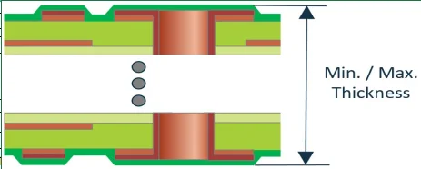 |
|
Min thickness
|
0.12mm (2L)
0.18mm (4L) |
||
|
Tolerance
|
Thickness≤1mm: ±0.1mm
Thickness>1mm: ±10%C |
 |
|
|
Finished PCB
length
|
Max length
|
1100mm
|
|
|
Min length
|
10mm
|
||
|
Finished PCB width
|
Max width
|
570mm
|
|
|
Min width
|
Relay VCC
|
||
|
Surface Finish
|
Sn thickness of HASL/LF-HASL
|
2-40um (0.4um on large Tin area of leaded HASL, 1.5um on large Tin area of lead-free HASL)
|
|
|
Min space between pads for HASL/LF-HASL PCB without solder mask
|
0.175mm (Pad space 0.25mm in large copper areas)
|
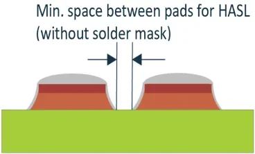 |
|
|
OSP thickness
|
0.2-0.6um
|
||
|
ENIG thickness
|
Ni: 3-8um; Au: 0.05-0.1um
Cannot do 0.08um min gold |
||
|
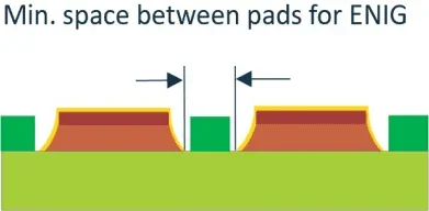
Min space between pads for ENIG PCB
|
0.08mm (base copper 1/3 oz, 0.5 oz)
|
 |
|
|
Immersion Silver
|
0.15-0.4um
|
||
|
Immersion Tin
|
≥1.0um
|
||
|
Hard gold
|
0.1-4.0um
|
||
|
Soft gold
|
0.1-4.0um
|
||
|
ENEPIG
|
Ni: 3-8um, Pd: 0.05-0.15um, Au: 0.05-0.1um
|
||
|
Flash gold(electroplated gold)
|
Ni: ≥3um; Au: 0.025-0.1um; base copper≤1oz
|
||
|
Electroplated Gold finger
|
Ni:≥3um; Au: 0.25-1.5um (the thinnest point)
|
||
|
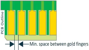
Min space between gold fingers
|
Dry film pattern plating 0.175mm; lead process 0.125mm
|
 |
|
|
ENIG+Gold finger
|
Yes (need line)
|
||
|
Flash gold(electroplated gold)+Gold finger
|
Yes
|
||
|
Immersion silver+gold finger
|
Yes (need line)
|
||
|
Immersion tin+gold finger
|
Yes (need line)
|
||
|
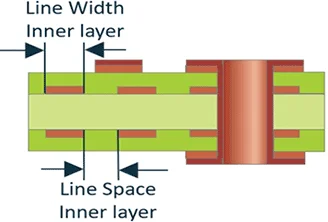
Inner layer
line width/space
|
1/2OZ Limit
Normal |
3/3mil
|
 |
|
1OZ Limit
Normal |
3/4mil
|
||
|
2OZ Limit
Normal |
4/5mil
4/5.5mil |
||
|
3OZ Limit
Normal |
5/8mil
5/8mil |
||
|
4OZ Limit
Normal |
6/11mil
6.5/11mil |
||
5OZ Limit
Normal |
7/13.5mil
7/14mil |
||
|
6OZ Limit
Normal |
8/15mil
8/16mil |
||
|
7OZ Limit
Normal |
9/10mil
|
||
|
8OZ Limit
Normal |
9/10mil
|
||
|
9OZ Limit
Normal |
12/10mil
|
||
|
10OZ Limit
Normal |
12/10mil
|
||
|
11OZ Limit
Normal |
15/25mil
|
||
|
12OZ Limit
Normal |
15/25mil
|
||
|
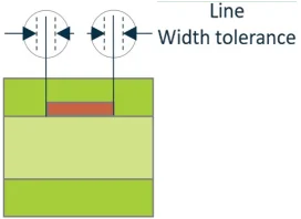
Tolerance
|
≤10mil: ±1.0mil, ±1mil
>10mil: ±1.5mil, ±20% |
 |
|
|
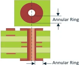
Inner layer
annular ring
|
1/2OZ
|
6.5mil
|
 |
|
1OZ
|
7mil
|
||
|
2OZ
|
7mil
|
||
|
3OZ
|
8mil
|
||
|
4OZ
|
8mil
|
||
|
5OZ
|
9mil
|
||
|
6OZ
|
NA
|
||
|
7OZ
|
NA
|
||
|
8OZ
|
NA
|
||
|
9OZ
|
NA
|
||
|
10OZ
|
NA
|
||
|
11OZ
|
NA
|
||
|
12OZ
|
NA
|
||
|
Inner layer
grid
|
1/2OZ |
8/8mil
|
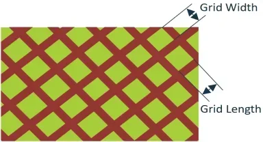 |
1OZ |
10/10mil
|
||
2OZ |
12/12mil
|
||
3OZ |
Yes, not defined
|
||
4OZ |
Yes, not defined
|
||
5OZ |
Yes, not defined
|
||
6OZ |
Yes, not defined
|
||
7OZ |
NA
|
||
8OZ |
NA
|
||
9OZ |
NA
|
||
10OZ |
NA
|
||
11OZ |
NA
|
||
12OZ |
NA
|
||
|
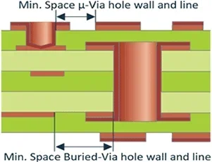
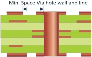
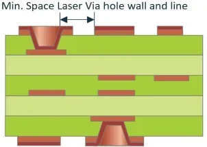
Min space between hole wall and conductor
|
Min space between hole wall and conductor (mechanical blind and buried vias and 2+2+2 laser buried and blind vias)
|
0.175mm (normal 0.2mm) for one-time laminating, 0.2mm (normal 0.225mm) for two times laminating, 0.225mm for three times laminating
|
 |
|
Min space between hole wall and conductor (None blind and buried vias and 1+N+1 laser blind via)
|
0.1375mm (normal 0.175mm) (≤8L), 0.1625mm (normal 0.2mm) (10-14L), 0.175mm (normal 0.2mm) (>14L)
|
 |
|
|
Min space between laser holes and conductor (1+N+1 and 2+N+2 HDI PCB)
|
0.05mm (PTH PCB)
|
 |
|
|
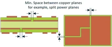
Min width of internally isolated strip
|
0.2mm
|
 |
|
|
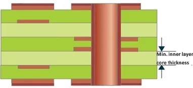
Min inner layer core thickness
|
Relay VCC
|
 |
|
|
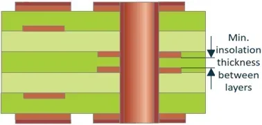
Lamination
|
Min isolation thickness between layers
|
0.05mm (just for base copper 0.5 oz)
|
 |
|
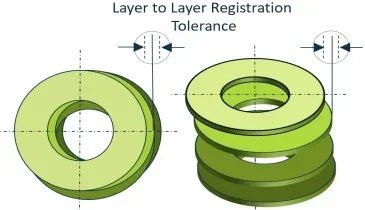
Layer-to-layer registration tolerance (mm)
|
0.125mm (normal 0.15mm)
|
 |
|
|
Hole
|
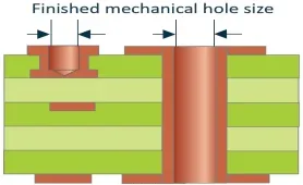
Finished mechanical hole size
|
0.1-6.1mm (corresponding drilling tool size 0.15-6.2mm)
|
 |
|
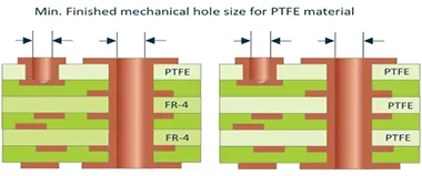
Min finished hole size for PTFE material and hybrid PTFE PCB
|
0.25mm
|
 |
|
|
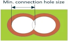
Min connecting hole size
|
0.35mm (corresponding drilling tool size is 0.45mm)
|
 |
|
|
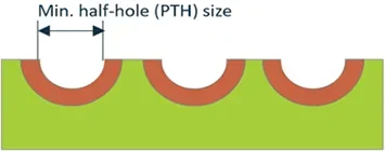
Min half-hole (PTH) size
|
0.3mm (corresponding drilling tool size is 0.4mm)
|
 |
|
|
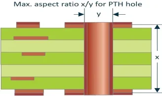
Max aspect ratio for PTH hole
|
20: 1 (hole diameter>0.2mm)
|
 |
|
|
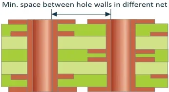
Min space between hole walls in different nets after compensation
|
0.25mm
|
 |
|
|
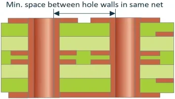
Min space between hole walls in the same net after compensation
|
0.15mm (PTH-hole & laser hole PCB),
0.25mm (Mechanical blind & buried hole PCB)
|
 |
|
|
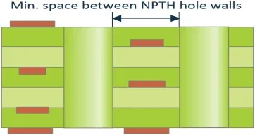
Min space between NPTH hole walls
|
0.2mm
|
 |
|
|
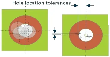
Hole location tolerance (compared with CAD data)
|
±0.05mm
|
 |
|
|
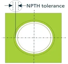
NPTH tolerance
|
±0.05mm
(limit +0/-0.05mm or +0.05/-0mm)
|
 |
|
|
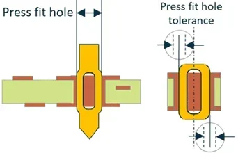
Pressfit hole tolerance
|
±0.05mm
+0.06/-0.04mm |
 |
|
|
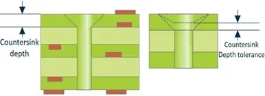
Countersink depth tolerance
|
±0.15mm
|
 |
|
|
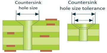
Countersink hole size tolerance
|
±0.15mm
|
 |
|
|
Countersink size and angle
|
PTH and NPTH, special: 82°, 90°, 120°, 135° (countersink drilling size 12-393.7mil)
|
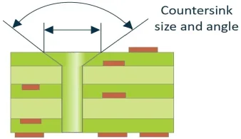 |
|
|
PTH and NPTH, standard: angle130° (drilling size≤125mil), 165°(drilling size 125--248mil)
|
|||
|
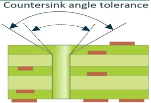
Countersink angle tolerance
|
±10°
|
 |
|
|
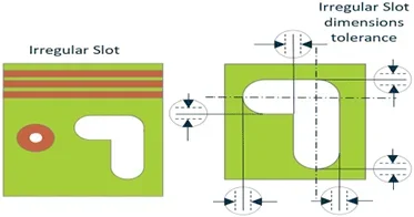
Irregular slot tolerance (routing holes)
|
±0.1mm
normal ±0.125mm |
 |
|
|
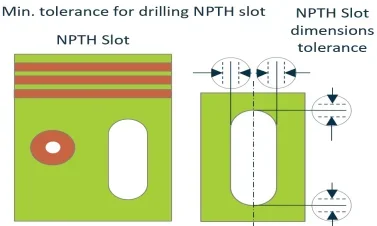
Min tolerance for drilling slot
|
NPTH slot:
Length/width≥2, width ±0.05mm, and length tolerance ±0.05mm; Length/width<2, width ±0.075mm, and length tolerance ±0.075mm
|
 |
|
|
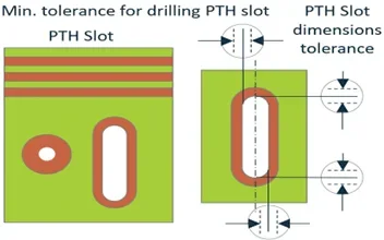
PTH slot:
Length/width≥2, width ±0.075mm, and length tolerance ±0.075mm; Length/width<2,width ±0.075mm, and length tolerance ±0.1mm
|
 |
||
|
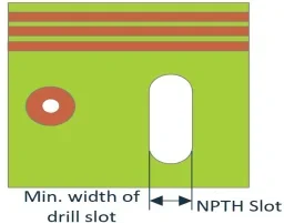
Min width of drill slot
|
0.45mm
|
 |
|
|
Backdrilling
|
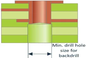
Drill hole size for backdrilling
|
0.5-6.2mm
|
 |
|
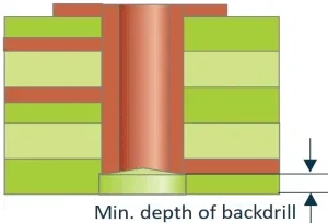
Min. depth of backdrilling
|
0.2mm
|
 |
|
|
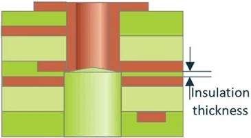
Insulation thickness between backdrilling layers (backdrilling target layer that must be cut & the next layer that must not cut
|
≥0.2mm
|
 |
|
|
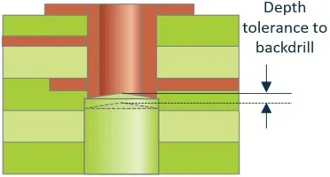
Depth tolerance to backdrilling
|
±0.1mm
|
 |
|
|
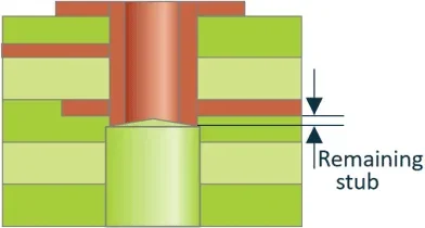
Stub (Copper barrel that remains after backdrilling, measured from the must-not-cut layer)
|
Not defined
|
 |
|
|
Pad (ring)
|
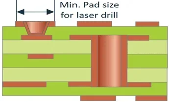
Min Pad size for laser drill
|
Hole diametrer D+0.15mm
|
 |
|
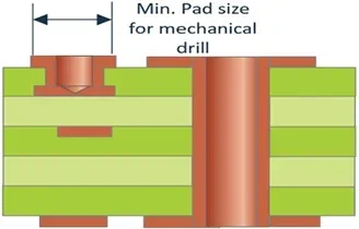
Min Pad size for mechanical drilling
|
Hole diametrer D+0.2mm
|
 |
|
|
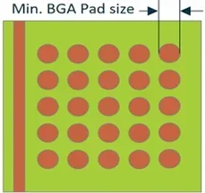
Min BGA pad size
|
HASL: 0.25mm,
LF HASL: 0.3mm, Other surface finishes: 0.175mm |
 |
|
|
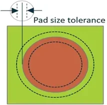
Pad size tolerance (BGA)
|
±0.03mm (pad size≤0.3mm);
±10% (pad size≥0.3mm) |
 |
|
|
Outer layer
line width/space
|
1/3OZ: Best
Normal |
3.0/3.0mil
3.5/3.5mil |
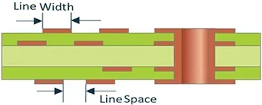 |
|
1/2OZ: Best
Normal |
3.5/3.6mil
4/4mil |
||
|
1OZ: Best
Normal |
4/4.5mil
5/5mil |
||
|
2OZ: Best
Normal |
5/6mil
7.5/8mil |
||
|
3OZ: Best
Normal |
6/7.5mil
9.5/10mil |
||
|
4OZ: Best
Normal |
14/12mil
14/14mil |
||
|
5OZ: Best
Normal |
18/17mil
18/18mil |
||
|
6OZ: Best
Normal |
20/24mil
22/26mil |
||
|
7OZ: Best
Normal |
22/26mil
24/28mil |
||
|
8OZ: Best
Normal |
Yes
|
||
|
9OZ: Best
Normal |
Yes
|
||
|
10OZ: Best
Normal |
Yes
|
||
|
11OZ: Best
Normal |
Yes
|
||
|
>=12OZ: Limit
Normal |
Yes
|
||
|
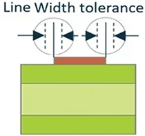
Width tolerance
|
±20%
(Impedance boards ±10%) |
 |
|
|
Outer layer
grid
|
1/3OZ
|
6/6mil
|
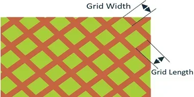 |
|
1/2OZ
|
6/6mil
|
||
|
1OZ
|
6.5/6mil
|
||
|
2OZ
|
10/11mil
|
||
|
3OZ
|
10/13mil
|
||
|
4OZ
|
12/16mil
|
||
|
5OZ
|
Yes
|
||
|
6OZ
|
Yes
|
||
|
7OZ
|
NA
|
||
|
8OZ
|
NA
|
||
|
9OZ
|
NA
|
||
|
10OZ
|
NA
|
||
|
11OZ
|
NA
|
||
|
12OZ
|
NA
|
||
|
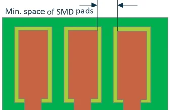
Min space of SMD pads (requiring solder mask
bridge) before compensation
|
1/3 OZ base copper
|
Not defined
|
 |
|
1/2 OZ base copper
|
Limit: 7.2mil (black sm: add 1.5mil, immersion tin: add 2mil, on ground copper area: add 4mil)
|
||
|
1 OZ base copper
|
Limit: 8mil (on ground copper area: add 4mil)
|
||
|
2 OZ base copper
|
Limit: 11mil (on ground copper area: add 2mil)
|
||
|
3 OZ base copper
|
Limit: 12mil (on ground copper area: add 2mil)
|
||
|
4 OZ base copper
|
Not defined
|
||
|
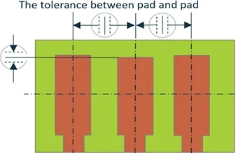
Position tolerance
|
Tolerance between pad and pad (Fiducial mark pad to Fiducial mark pad)
|
L≤300mm: ±0.1mm
L>300mm: ±0.125mm |
 |
|
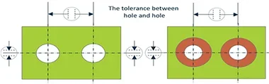
Tolerance between Hole and Hole
|
NA
|
 |
|
|
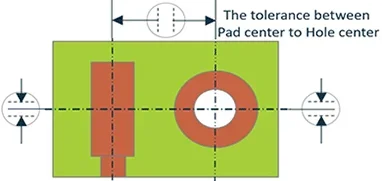
Tolerance between Pad center to Hole center
|
NA
|
 |
|
|
Via filling with resin for Via in PAD (POFV/ VIPPO)
|
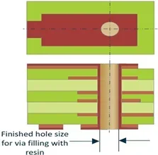
Finished hole size for via filling with resin
|
0.1-0.9mm (drill size 0.15-1.0mm),
0.3-0.55mm normal (drill size 0.4-0.65mm) |
 |
|
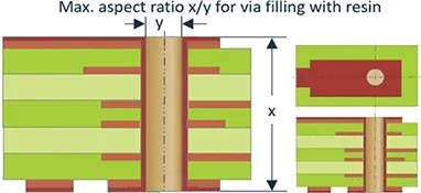
Max aspect ratio for via filling with resin PCB
|
12: 1
|
 |
|
|
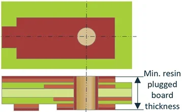
Min resin plugged PCB thickness
|
0.2mm
|
 |
|
|
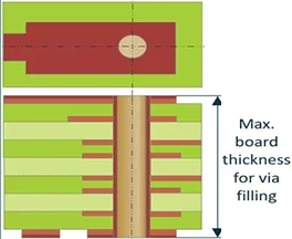
Max via-filling-with-resin PCB thickness
|
3.2mm
|
 |
|
|
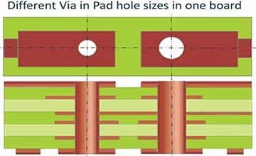
Can you make different hole sizes in one board?
|
Yes
|
 |
|
|
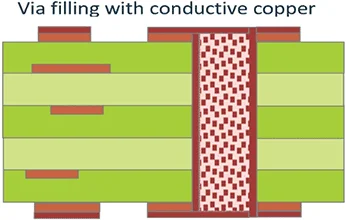
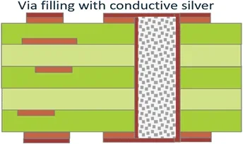
Via filling with conductive copper paste/Silver paste
|
Via filling with conductive copper filling
|
Yes
|
 |
|
Via filling with conductive silver filling
|
Yes
|
 |
|
|
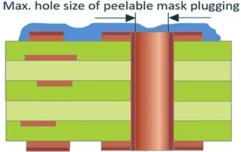
Peelable mask
|
Max hole size of peelable mask plugging
|
5mm
|
 |
|
The thickness of peelable mask
|
0.2-0.78mm
|
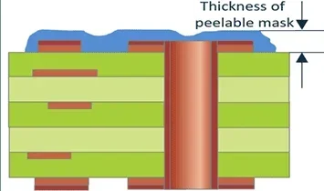 |
|
|
Min space between Peelable soldermask and pads
|
0.35mm
|
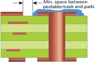 |
|
|
Peelable solder mask larger than pad size (single-sided)
|
0.3mm
|
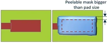 |
|
|
Carbon ink
|
Carbon ink thickness
|
10-50um
|
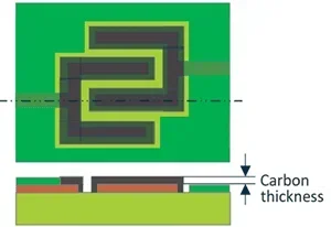 |
|
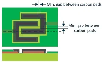
Min gap between carbon pads
|
0.325mm
|
 |
|
|
Carbon ink with resistance control
|
NA
|
||
|
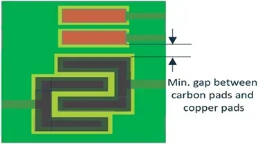
Min gap between carbon and pads
|
0.2mm
|
 |
|
|
Solder mask
|
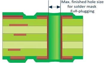
Max finished hole size for solder mask full-plugging (both sides without solder mask opening)
|
0.8mm
|
 |
|
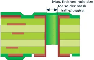
Max finished hole size for solder mask half-pugging (one side with solder mask opening, the other side without)
|
0.45mm
|
 |
|
|
Solder mask color
|
Green matte/glossy, yellow, black, blue, red, white
|
||
|
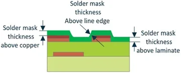
Solder mask thickness
|
10-18um (on copper area),
5-7um (on via pad), ≥5um (on circuits around the corner, just for one-time print and copper thickness<48um) |
 |
|
|
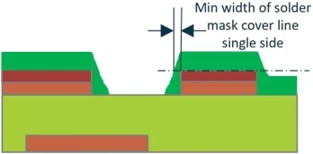
Min width of soldermask cover line single side
|
2.5mil (partial area can be allowed 1.5mil)
|
 |
|
|
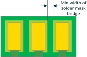
Min width of solder mask bridge
|
a. Base copper≤0.5 oz: Immersion Tin: 7.5mil (black), 5.5mil (other color); other surface treatment: 5.5 mil (black,extremity 5mil), 4mil (other color,extremity 3.5mil)
b. Base coppe 1 oz: 4mil (green), 5mil (other color), 5.5mil (black, extremity 5mil) c. Base copper 1.43 oz: 4mil (green), 5.5mil (other color), 6mil (black) d. Base copper 2 oz-4 oz: 6mil |
 |
|
|
Silkscreen color
|
White, yellow, black |
||
|
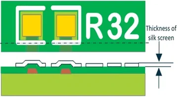
Silkscreen thickness
|
Not defined
|
 |
|
|
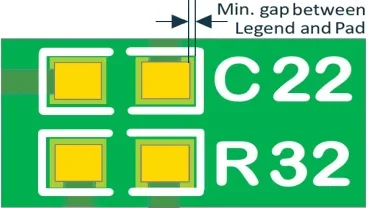
Min gap between Legend and Pad
|
6mil (PTH & laser hole PCB),10mil (mechanical blind & buried PCB)
|
 |
|
|
Silkscreen print type (only for white color)
|
Serial number, barcode, planar code
|
||
|
QR code scan
|
By Printer
|
||
Now you've learned about all the rigid PCB capabilities of PCBONLINE. Besides rigid PCBs, PCBONLINE also provides flexible PCBs and rigid-flex PCBs, and we will publish the other two blog pages for you to fully understand what PCBONLINE can do in PCB manufacturing.
If you find PCBONLINE matches your project manufacturing demands, don't hesitate to email info@pcbonline.com to get a quote.
PCB fabrication at PCBONLINE.pdf


