

PCBONLINE is an advanced PCB manufacturer founded in 2005. Over the past two decades, it has built three PCB and PCBA manufacturing bases: one PCB factory in Jiangxi, one PCB factory in Jiangsu, and one PCB assembly factory in Shenzhen. All levels of production, from prototypes to large-scale manufacturing, happen on the same production lines. You may be curious - what are the manufacturing capabilities of PCBONLINE?
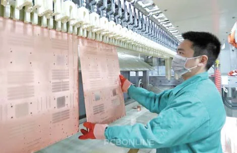
First, let's look into the PCB manufacturing capabilities. PCBONLINE focuses on high-end PCBs, such as flexible (FPC), rigid-flex PCBs, HDI, etc. Below are its PCB fabrication and assembly capabilities:
PCB Manufacturing Capabilities
We classify the printed circuit boards into HDI boards and plated through-hole boards. Here are the PCB manufacturing capabilities at PCBONLINE.
|
Technical Capabilities
|
Plated Through-Hole Boards
|
|
|
Maximum Layers
|
64
|
64
|
|
HDI Stackup
|
4+N+4
|
/
|
|
Max. Processing Board Size
|
24.5" × 28.5" (620 × 720mm)
|
24.5" × 37.5" (620mm × 950mm)
|
|
Min. Line Width/Line Space
|
I/L: 2.5mil/2.5mil O/L: 4mil/4mil (POFV)
|
I/L: 2.5mil/2.5mil O/L: 4mil/4mil(POFV)
|
|
Board Thickness
|
3.5mm
|
4.0mm
|
|
Min. Drill Bit
|
6mil
|
6mil
|
|
Aspect Ratio
|
18:01
|
18:01
|
|
Min. Micro Via & Aspect Ratio
|
4mil & 0.8:1
|
/
|
|
Min Core Board Thickness
|
2mil
|
2mil
|
|
Alignment between Layers
|
5mil
|
5mil
|
|
Solder Mask Tolerance
|
±8%
|
±8%
|
|
Back Drill stub
|
2-10mil
|
2-10mil
|
|
Copper Fill
|
Yes
|
/
|
|
POFV
|
Yes
|
Yes
|
|
Skip-via (L1-3)
|
No
|
No
|
|
Buried Copper Block
|
Yes
|
Yes
|
|
Buried Capacitance
|
No
|
No
|
Please note that plated through-hole PCBs in our chart include many types of PCBs, such as high-frequency, ceramic, thick-copper, high-TG, halogen-free, etc. I will add all the specific specification charts of these advanced boards to this post when I am done.
Let's see the details of back-drilling PCB capabilities.
Back Drilling PCB Capabilities
|
Technical Specifications
|
Diagrammatic Sketch
|
Back Drill PCB Capabilities
|
|
Drill hole size for back-drilling
|
 |
0.5mm-6.2mm |
|
Min. depth of backdrill
|
 |
0.2mm |
|
Insulation thickness between backdrill layers & next layer(backdrill target layer that must be cut & the layer that must not be cut)
|
 |
≥0.2mm |
|
Depth tolerance to Backdrill
|
 |
±0.1mm |
|
Stub (Copper barrel that remains after back drill, measured from the must-not-cut layer)
|
 |
no define
|
Let's see PCBONLINE's capabilities for flexible PCBs.
Flexible PCB Capabilities
|
Technical Specifications
|
Flexible PCB Capabilities
|
|
Layer Count
|
1-8L
1-4 L (normal) |
|
PCB thickness
|
0.1-0.5mm (1-4L)
0.6-0.8mm (5-8L) |
|
The tolerance of flex PCB thickness (≤0.3mm) (exclude stiffener)
|
±0.03mm
|
|
The tolerance of multilayer flex PCB thickness (≤0.3mm-0.8mm) (exclude stiffener)
|
±10%
|
|
The tolerance of flex PCB thickness (include PI/FR4 stiffener)
|
±10%
|
|
Maximum finished flex PCB size
|
7.8inch*21.8inch(PI≥1mil)
7.8inch*14inch (normal) |
|
Minimum finished flex PCB size
|
2mm*4mm (no connection tab)
8mm*8mm (with connection tab) |
|
Minimum Line Width/Line Space
|
0.035mm/0.035mm
|
|
Min. Interlayer Alignment
|
±0.05mm
|
|
Min. Hard Board Dielectric Layer Thickness
|
/
|
|
Surface Finishes
|
ENIG, OSP, ENEPIG, Immersion Tin
|
|
Applications
|
display module, smartphone, camera module, consumer electronics
|
Let's see PCBONLINE's capabilities for rigid-flex PCBs.
Rigid-Flex PCB Capabilities
|
Technical Specifications
|
Rigid-Flex PCB Capabilities
|
|
Maximum Layers
|
24
|
|
Flex Layer Count
|
11-20L (18L)
|
|
Min. Laser Blind Hole Aperture
|
0.1mm
|
|
Flex layer on outer or Middle Layer
|
Middle
|
|
Finished PCB thickness
|
0.2mm-4.0mm
|
|
Tolerance of PCB thickness
|
>1.0mm, ±10%
≤1.0mm, ±0.1mm |
|
Min flex layer width
|
2.5mm
|
|
Min flex layer width between rigid
|
3mm
2mm(limit) |
|
Maximum PCB panel size
|
406mm*736mm
|
|
Minimum PCB panel size
|
10mm*15mm
|
|
Impedance tolerance
|
Single-ended: ±3Ω(≤50Ω), ±8%(>50Ω)
Differential pair: ±4Ω (≤50Ω), ±8%(>50Ω) |
|
HDI type
|
3+n+3 (n buried hole≤0.4mm)
|
|
Minimum twist & warpage
|
0.75%(symmetrical
1.5%(asymmetrical) |
|
Adhesive dispense width
|
1.5±0.5mm (slot width≥5mm)
|
|
Min distance between R-F connect area and conductor
|
0.3mm(half depth slot process)
0.5mm normal |
|
Min. width of resin flow out in R-F connect area
|
0.5mm
1.0mm normal |
|
Min distance between E-test pads
|
3mil
4mil normal |
|
Min BGA pad size BGA
|
10mil (electrical Ni/Au7mil)
12mil (electrical Ni/Au8mil) normal |
Let's see the details of metal (aluminum/copper) core PCB capabilities.
Aluminum and Copper-Core PCB Capabilities
|
Technical Specifications
|
Diagrammatic Sketch
|
Metal-Core PCB Capabilities
|
|
Layer count for aluminum PCB
|
/
|
1-4L |
|
Layer count for copper-core PCB
|
/
|
1-8L |
|
Maximum PCB size
|
/
|
500mm*1200mm |
|
Finished PCB copper thickness
|
 |
0.5oz-4oz |
|
Metal base thickness(alu/copper)
|
 |
0.8-2.6mm
|
|
Thermal prepreg (dielectric layer)) thickness
|
 |
0.05mm-0.2mm
|
|
Thermal conductivity
|
/
|
0.5w/m.k-6w/m.k
|
PCBONLINE's target customers are senior engineers, original equipment manufacturers, business makers, research institutes, and electronic solutions companies. If you are looking for a long-term PCB manufacturer for your devices, contact us by email at info@pcbonline.com.
PCB Assembly Capabilities
PCBONLINE has mature SMT, THT, and DIP lines for advanced PCB assembly. Our one-to-one engineering support, BOM and component inspection, and first-piece test will make sure the assembly's success.
The image below shows the functional mounting machine used in PCBONLINE's assembly factory. Functional mounting machines are used to mount components of big sizes, such as BGA, FPGA, etc. Its capabilities can cover part of the PCB assembly capabilities:

|
Specifications
|
Values
|
|
Placement Accuracy
|
±0.035mm (Cpk≥1)
|
|
Placement Speed
|
42,000CPH
|
|
Feeder Inputs
|
Max. 112
|
|
Min. Board Size
|
50mm * 50mm
|
|
Max. Board Size
|
1,200mm * 370mm
|
|
Max. Rectangular Part Size
|
50mm * 150mm
|
|
Max. Square Part Size
|
74mm * 74mm
|
|
Max. Component Height
|
25mm
|
|
PCB Thickness
|
0.3mm - 4.0mm
|
|
Min. Component Size
|
0201mm
|
No matter what the circuit board quantity is, our manufacturing standards and procedures are the same. We never reduce PCB quality. Our strong manufacturing capabilities can meet all your requirements. If you have not worked with PCBONLINE, welcome to get a quote online or contact us. Our circuit board quality will meet and exceed your expectations.
PCB assembly at PCBONLINE.pdf


