
Rigid-flex PCB is one of the most advanced and high-performance circuit boards ever. Since you spend money on rigid-flex PCB manufacturing, you have all the reasons to know how your boards are manufactured in PCB factories.
You can get to know the following from this article:
Part 1. Key Step in Rigid-Flex PCB Manufacturing
The key step of rigid-flex PCB manufacturing is removing the redundant rigid materials from the flexible layers.
![]()
For example, the above rigid-flex PCB is manufactured by laminating 4 rigid circuit layers on 2 flexible layers and then laser cutting excessive rigid prepreg bonded to the desired flex section by laser.
In this way, the flex section (layers 3 and 4) is exposed. We get a rigid-flex PCB that is composed of 2 flex PCB layers and 4 rigid FR4 PCB layers.
Knowing this, you will find it easier to understand the rigid-flex PCB manufacturing process below.
Part 2. Step-by-Step Rigid Flex PCB Manufacturing Process
Step 1. Rigid-flex PCB material preparation
![]()
Before rigid-flex PCB manufacturing, we need to pre-clean the flexible copper-clad laminates (FCCL) and cut the chemically-cleaned FCCL, polyimide (PI), prepreg, and coverlay into the desired width.
Step 2. Generating the inner core for the flex section
Rigid-flex PCB manufacturing starts from the internal flex board, and flex board manufacturing starts from generating the flex inner core. PI is the base material of the flex core.
If the rigid-flex design has one flex layer:
We laminate a thin copper foil on the PI.
If the rigid-flex design has two or more flex layers:
We laminate two external copper foils on PI.
Step 3. Generating circuits on flex inner core
The purpose of this step is to leave copper lines in the circuit pattern on the copper foil and remove other copper.
First, the copper foil is coated with a photoresist that can cure when UV light irradiates it.
Then, we place a nontransparent film that draws the transparent PCB circuits on the copper foil.
![]()
Then we turn on the UV light. In this way, copper in the PCB circuit pattern is covered and protected by the cured dry film.
Next, we wash away the photoresist that is not cured with the chemical solution.
Next, we use NaOH to solve the copper that is exposed. In this way, only the copper circuit traces are left on the inner core.
Step 4. Laminating, circuits generation, and drilling on Flex Section
Here are two cases:
If the rigid-flex design has more than two flexible layers, we laminate alternating layers of PI and copper foil on the flex inner core. Then we start to generate circuits.
If the rigid-flex design has one or two flexible layers, we directly go to the next process.
Circuit generation on external flex layers: this is similar to the last step, but the difference is that we remove copper in the PCB circuit pattern and keep the other copper.
Then the circuit area is electroplated first with copper and then with tin.
Then we peel off the photoresist and use NaOH to etch away the copper in the non-circuit area, while the circuit area is protected by tin.
Next, the tin is also removed. And now, only the electroplated copper circuit traces are kept on external flex layers.
![]()
Laser drilling: We drill plated-through holes on the flex layers by laser.
Finally, we laminate the coverlay on the flex layers.
Now, the flex region has been completed.
Step 5. Laminating, circuit generation, and drilling on rigid layers
Here are two cases: plated-through holes and HDI.
Rigid-flex PCB with plated-through holes: we laminate alternating layers of prepreg and copper foil on the flex region. Complete circuit generation and drilling as Step 4. The only difference is that it is mechanical drilling.
Rigid-flex PCB with HDI requirements: we laser-drill mircovias on the alternating layer of prepreg and copper foil.
And we laminate the alternating layers on the flex section.
Then we generate circuits on the rigid layers as in Step 3.
Step 6. Laser-cut off the redundant prepreg outside the flex region
![]()
Here we use the laser to cut off the non-circuit prepreg area in the rigid layers so that the desired flex section is exposed.
At PCBONLINE, the laser cut is smart and accurate. It won’t hurt the coverlay of the flex section.
Step 7. Complete rigid-flex PCB manufacturing and testing
Then we treat the edge of the panel, such as V-cut, half holes, etc.
Finally, we test the rigid-flex PCB. The main tests are flying probe and nail-in-bed. If rigid-flex PCBs are used in automotive, medical, defense, and aerospace industries, they should also pass the four-terminal sensing test.
Voila, the above is the complete rigid-flex PCB manufacturing process. If you have any concerns about rigid-flex PCB manufacturing, please feel free to let us know. You can contact us from the online window on the right of the screen.
Part 3. Why PCBONLINE
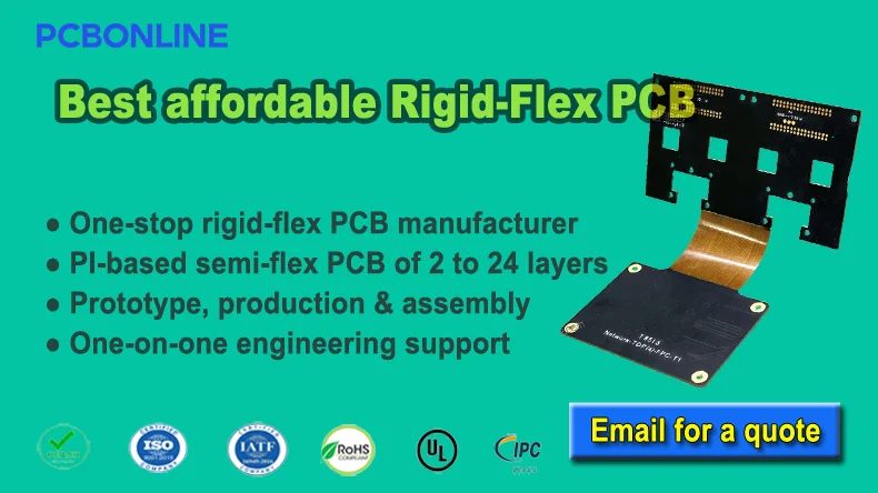
PCBONLINE is a one-stop rigid-flex PCB manufacturer that has passed ISO, IATF, REACH, UL, and RoHS certifications. If you are looking for reliable and high-quality rigid-flex PCB manufacturing, choose to work with PCBONLINE.
The reasons to have rigid-flex PCBs manufactured from PCBONLINE are:
- Strong rigid-flex PCB manufacturing capabilities - flex section from 1 to 6 layers, rigid section from 2 to 24 layers
- HDI capabilities from 1+N+1 to 4+N+4 for rigid-flex PCB manufacturing
- One-on-one engineering support with free DFM, DFT, and DFX for your rigid-flex project
- Fast rigid-flex PCB manufacturing time - from 1 to 4 weeks, and delivery time from 2 to 3 days
- Very fair rigid-flex PCB prices. Welcome to quote, which is quick and free!
Here you can check the rigid-flex PCB manufacturing capabilities from PCBONLINE:
|
Features
|
PCBONLINE's Rigid-Flex PCB Manufacturing Capabilities
|
|
Layers
|
rigid section: 2 to 24, flex section: 1 to 6
|
|
Build time
|
1 day to 4 weeks
|
|
Board size
|
Min. 4mm×4mm to Max. 457mm×610mm
|
|
Final board thickness
|
0.05mm to 0.6mm
|
|
Materials
|
Polyimide, high TG polyimide, FR4, FR4 high TG, RA copper, HTE copper, adhesive
|
|
PCB thickness in flex section
|
0.01mm to 0.15mm
|
|
Min. pitch
|
0.35mm
|
|
HDI stack-up
|
1+N+1, 2+N+2, 3+N+3, 4+N+4
|
|
Stiffener
|
FR4, PI, stainless steel
|
|
Aspect ratio
|
1:3
|
|
Copper thickness
|
1/3oz to 3oz
|
|
Min. track/space
|
1.6mil/1.6mil
|
|
Min. mechanical drilling Ø
|
6mil
|
|
Hole size tolerance
|
PTH: ±2mil, NPTH: ±1mil
|
|
Hole position tolerance
|
±2mil
|
|
Surface finishes
|
ENIG: Au 1µ to 5µ", Ni 80µ to 200µ"
OSP
Immersion tin: 0.8µm to 1.2µm
Immersion silver: 0.15µm to 0.45µm
Hard gold plating: Au 1µ to 50u", Ni 80µ to 200µ"
|
Conclusion
This article reveals the most complete rigid-flex PCB manufacturing process from PCBONLINE. I hope you can get a clear insight into rigid-flex PCB manufacturing from this article. If you want to turn your creativeness in rigid-flex design into reality, do not miss the 20-year-old source factory PCBONLINE.


