
A high-frequency microwave PCB is a specialized PTFE circuit board designed for frequencies surpassing 1GHz. While not as commonly recognized as smartphones or laptops, microwave PCBs play a significant role in various advanced electronic systems in defense, aerospace, automotive, and medical applications.
In this article, we will be delving into the world of Microwave Printed Circuit Boards (PCBs) by exploring microwave PCB design challenges and the factors of consideration in selecting material for these PCBs. We also introduce a reliable microwave PCB manufacturer that offers high-quality manufacturing and ODM(original design manufacturing)/EMS(electronic manufacturing service) solutions.
What do You Know about Microwave PCB?
Microwave PCBs are high-frequency PCBs designed to operate with high-frequency signals within the RF and microwave frequency range. The ultimate aim of microwave PCB is minimal signal loss and optimal signal integrity.
Microwave PCBs are commonly used in systems like satellite communication, wireless communication, and other high-frequency electronic applications. Developing and manufacturing RF microwave PCBs demands specialized expertise and experience to guarantee the desired performance.
Microwave PCBs are characterized to handle microwave signals. These signals rang over 1 GHz frequency. It is because of these frequencies that specialized components are used in these PCBs that are capable of working with high-frequency signals.
The microwave PCB designs are distributed parameters circuits that tend to generate skin effect and coupling effect.
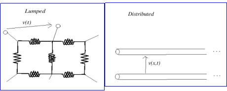
Figure 1
Unlike the lumped-element model, where passive electrical components like resistance, capacitance, and inductance are treated as concentrated at a single point in space, as shown in Figure 1, the distributed-element model considers the spatial distribution of these elements throughout the circuit as demonstrated in Figure 1. This model is particularly relevant in high-frequency applications and situations where the physical dimensions of the circuit elements are comparable to the wavelength of the signals involved.
Challenges in Microwave PCB Layout and Advice
Microwave PCB design is challenging due to the possible skin effect, coupling effect, and cross talk. Besides, microwave PCB has strict impedance control requirements. Below, we reveal the challenges in microwave PCB layout and give corresponding advice with intuitive drawings and explanations.
Skin Effect
For microwave PCB design, the conductor skin effect is a critical consideration, especially when operating frequencies increase. The skin effect is a phenomenon in which current (AC) tends to flow near the surface of a conductor, rather than uniformly throughout its cross-section as shown in Figure 2.
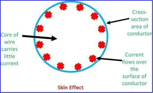
Figure 2
This phenomenon causes conductor resistance, leading to increased power dissipation and elevated temperatures thus impacting overall efficiency.
Addressing the skin effect is crucial in microwave PCB design to ensure optimal functionality and durability.
Various techniques and design strategies are used to alleviate the conductor skin effect in PCB design. PCB designers often try to keep the trace thickness (t) less than 0.1 times the skin depth (0.1×δ) to mitigate the skin effect, where δ represents the skin depth of the material.
Coupling Effect
The coupling effect in microwave PCB refers to unwanted signal interactions, particularly occurring at higher frequencies. Figure 3 shows the effect of coupling when two traces behave like a capacitor and as a result, the signal is distorted.
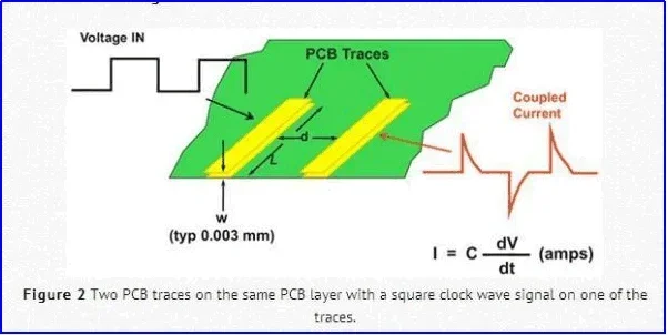
Figure 3
This phenomenon encompasses diverse forms of interference, such as capacitive or inductive coupling, especially in traces situated closely, shared ground planes, or neighboring components.
Employing design strategies like proper trace spacing, isolation of ground planes, and the implementation of controlled impedance is pivotal to mitigating the coupling effects in microwave circuits. Furthermore, the circuit layout must be turned with a 45-degree angle, which will help to reduce high-frequency signal emission and coupling between each other.
Electromagnetic Interference (EMI) and Radiation
Electromagnetic Interference encompasses conducted currents or radiated electromagnetic fields from a device. Most electromagnetic interference problems are associated with grounding, and bad grounding often starts in the PCB stack-up.
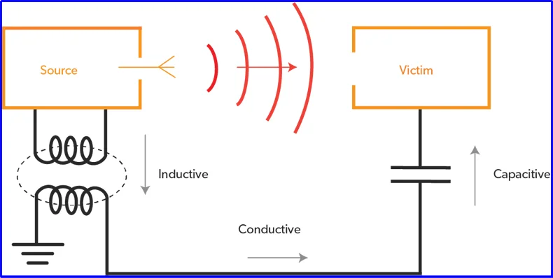
Figure 4
In Figure 4, we see a source and a victim line whose signals are interfered with due to electromagnetic induction.
Something as simple as including a ground plane and enforcing a single ground potential throughout a system prevents problems like the reception of electromagnetic interference.
Another tip to reduce signal interference refers to placing the layout between layers in the vertical direction, with the top layer in a horizontal direction, and the bottom layer in a vertical direction.
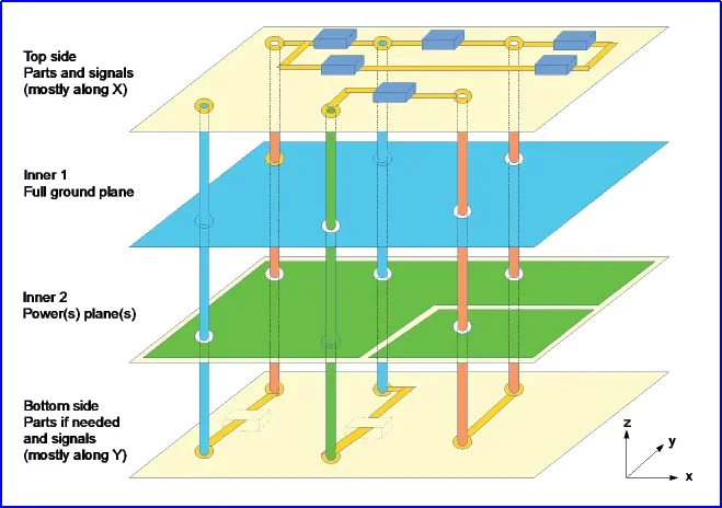
Figure 5
Figure 5 shows a multi-layer PCB along with the direction of routes in the top, bottom, and intermediate layers. Increasing copper on a ground layer to reduce the signal interference.
Impedance Control
The impedance of a microwave PCB is the combination of inductance and capacitance of the circuit while operating at microwave frequency. The impedance tolerance for microwave PCBs is a crucial need for maintaining signal integrity in high-frequency applications.
Commonly, the acceptable impedance tolerance is ±2% and below. It is necessary to control impedance in microwave PCBs to mitigate signal distortions, reflections, and other challenges linked to the conductor skin effect at microwave frequencies. This is essential for ensuring the utmost performance and reliability in the design of microwave PCBs.
In practical terms, impedance control for a trace is considered necessary only when the total length from the driver to the receiver surpasses 1/16th of the signal wavelength—this length is referred to as the critical length of the signal.
For instance, when routing a 1GHz signal, if the total length exceeds 425 mils, impedance control for that trace becomes essential. The controlled use of capacitors is emphasized to mitigate interference in impedance values.
Usually, capacitors cause interference that is why it is recommended that you either avoid using capacitors or place them in symmetry so that they can not interfere in the circuit impedance.
When capacitors are unavoidable, the symmetric placement is recommended ensuring signal unity across all traces.
Cross Talk
Cross talk refers to an excess of voltage or current of one trace inducing undesired effects on another trace, even when two are not physically connected. Crosstalk is a significant challenge in microwave circuit designs, primarily due to its direct correlation with the edge rates of the active line.
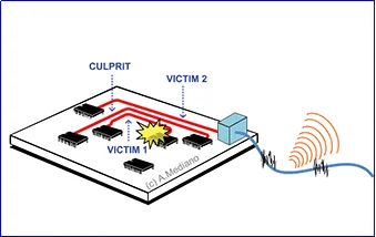
Figure 6
Figure 6 shows the crosstalk between a trace (culprit) affecting the other trace (victim). As PCB board densities rise, the issue of crosstalk becomes more pronounced and critical.
The use of the inner layer as a power ground layer, which will have the effect of shielding and shortening the length of the signal wire, reduces cross-interference between signals.
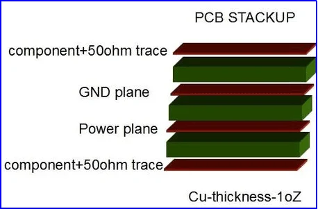
Figure 7
Figure 7 shows an example of a 4-layer PCB in which the power and ground layers are placed in between to avoid crosstalk.
The proper spacing of impedance-controlled traces and components is crucial to minimize crosstalk, with recommended minimum distances and isolation measures. A rule of thumb is to introduce a minimum distance between adjacent traces that is at least 3 times their width.
Factors to Consider in Materials for Microwave PCBs
Microwave PCB materials possess specific properties that represent their suitability for applications in printed circuits. When selecting a Microwave PCB laminate material, the dielectric constant (Dk) and dissipation factor (Df) are critical to consider.
Both Dk and Df play essential roles in material selection for PCBs tailored to the unique demands of diverse applications.
The dielectric constant (denoted as Dk) is a property that influences a material's capacity to store electrical energy within an electric field. Its impact extends to the speed of signal transmission through the PCB, governing both signal integrity and the characteristic impedance of transmission lines.
The dissipation factor (Df) is a critical parameter reflecting a material's efficiency in converting electrical energy into heat. In PCB applications, a preference for lower Df values is observed, aiming to minimize signal losses and ensure reliable performance.
For microwave applications, the PCBs should have low Df and Dk of 2 to 4 at 1MHz. For example, RO3003 has a DK of 3 and Df of 0.0013, and RO4350B has a DK of 3.66 and a Df of 0.0031.
In designing and production of microwave PCBs, other critical considerations include temperature stability, moisture and chemical resistance, radiation resistance, and signal integrity.
To ensure consistent performance, materials with low thermal expansion coefficients and stable electrical properties are chosen. Measures to resist moisture and chemicals, such as selecting appropriate substrate materials and implementing effective sealing, are essential.
In applications with radiation exposure, the selection of radiation-resistant materials and designs, along with shielding techniques, is crucial.
Maintaining signal integrity involves proper impedance matching, controlled dielectric constants, and minimizing signal losses.
The selection of substrate thickness in microwave PCBs is a critical design parameter, contingent on factors like operating frequency, dielectric constant, and application requirements. Typically, for microwave PCBs, substrates ranging from 10 mils to 125 mils are considered, with the optimal thickness determined by specific design goals.
For higher frequencies above 10 GHz, thinner substrates in the range of 10 to 20 mils are preferred to minimize signal losses and maintain signal integrity.
High-Quality Microwave PCB Manufacturing from Prototype to Bulk Production
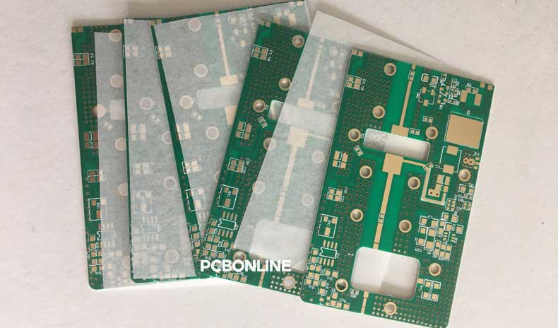
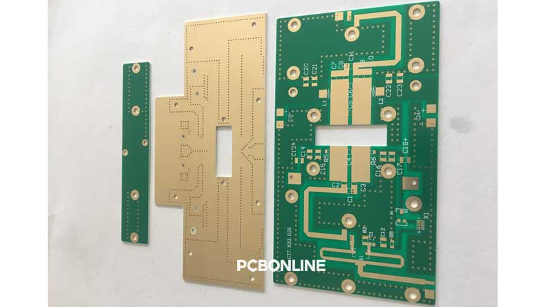
Microwave PCB manufacturing is also challenging for PCB manufacturers. The challenges include the in-stock laminates, strict impedance control, extremely small etching tolerance, the Plasma process, and the thermal shock test. If you have a plan for microwave PCB manufacturing, you can work with a reliable PCB manufacturer PCBONLINE that provides high-quality microwave PCB manufacturing from prototype to bulk production.
PCBONLINE is a one-stop PCB manufacturer for all types of high-frequency PCB, including microwave PCB, RF PCB, embedded antenna PCB, high-frequency MCPCB, Rogers/FR4/copper hybrid multilayer PCB, etc. Founded in 1999, PCBONLINE has two large advanced PCB manufacturing bases, one PCB assembly factory, and its R&D team to provide ODM/EMS solutions and engineering support.
Strong microwave PCB manufacturing capabilities, including trace width tolerance of +/-0.0007 inches and below, 100x microscope check for each circuit layer after etching, impedance tolerance of 2% and below, etc.
After drilling the PCB through holes, PCBONLINE has the Plasma process to remove drill dirt and any contaminants before copper plating to ensure manufacturing success.
PCBONLINE has in-stock high-frequency PCB laminates of all brands and models and can deliver microwave PCBs quickly.
All the microwave PCB laminates are stored within 45 days and are of high quality to ensure the best performance of the products.
PCBONLINE offers one-on-one engineering support and customer service throughout the project.
For bulk production, PCBONLINE provides the samples and PCBA functional testing for free.
PCBONLINE takes care of every detail of microwave PCB manufacturing and assembly to ensure the best quality and functionality of the PCB and product. It has rich production experiences in microwave PCB for military, aerospace, communications, automotive, and consumer electronics, such as radar systems, rockets, antennas, signal converter boards, Bluetooth devices, etc. If you want to get a quote from PCBONLINE, please contact us by email at info@pcbonline.com.
Conclusion
This article comprehensively unveils microwave PCB from design, and materials, to manufacturing. The challenges in microwave PCB layout are the skin effect, coupling effect, impedance control, EMI, and cross talk. The advice is given with drawings and examples, including 45-degree angles, keeping proper line thickness/width, isolating ground planes, layout between layers in the vertical direction, and avoiding using capacitors.
In selecting microwave PCB materials, the critical considerations include the DK, Df, temperature stability, and moisture and chemical resistance. For microwave PCB manufacturing and assembly, you can work with the advanced PCB manufacturer PCBONLINE, who provides one-stop and high-quality manufacturing.
PCB fabrication at PCBONLINE.pdf


