
High-frequency PCBs are PTFE-based printed circuit boards that transfer RF/microwave signals of 1 to 10 GHz. If you or your company/institute work in aerospace/defense/communication fields, designing high-speed/high-frequency PCBs is a must-have job for you.
No worries! There are useful design rules for high-frequency PCBs. Following these rules, you can design working high-frequency PCBs with your smart mind.
- Part 1: Challenges in High-Frequency PCB Designing
- Part 2: High-Frequency Design Rules in PCB Wiring
- Part 3: High-Frequency Design Rules in PCB Layers
- Part 4: High-Frequency PCB Design Rules for Grounding
- Part 5: High-frequency PCB Design Rules for Power Supply
- Part 6: It's Time to Check Your High-Frequency PCB Design
Basics for Designing High-Frequency PCBs
High-frequency PCBs are used to transmit and receive high-frequency signals. There are two antennas embedded into the circuit board as the radio frequency signal transmitter and receiver. The high-frequency circuit generates the RF waves and evaluates the reflected waves. The complete RF system is on the front side of the PCB. A high-frequency PCB also has a digital circuit to evaluate the RF signals, and it is on the backside of the circuit board.
Part 1: Challenges in High-Frequency PCB Designing
How to design high-frequency PCBs? First, let's understand the biggest challenge - crosstalk. Almost all design rules for high frequency in this article serve to reduce the crosstalk.
In high-frequency PCBs, RF/microwave signals transfer through the PCB wires as electromagnetic waves. The electromagnetic field is perpendicular to the PCB wire. If electromagnetic fields of different PCB wires couple, unwanted disturbance happens to the RF/microwave signals. This is the crosstalk.
Besides the crosstalk, take care of PCB wires' signal emission - we do not wish signal radiation from the PCB wires. Signals' external emission is unwelcome because it reduces the signal quality and causes disturbance to other signals. (Oh-oh! Signal external emission and crosstalk cause and affect each other.)
To solve the crosstalk and signals' external emission, design rulers for high-frequency are illustrated below. Let's begin!
Part 2: High-Frequency Design Rules in PCB Wiring
Rule No. 1: straight PCB wires with 45° corners and corners as few as possible
![]()
Look at this high-frequency PCB. You may notice that its PCB wires are straight, and the wires have 45° corners only when necessary. In a high-frequency PCB, the PCB wires are supposed to have continuous impedance, and we prefer straight lines. The PCB's designer uses straight wires and 45°corners as few as possible to reduce the external emission and mutual coupling of high-frequency signals. High-frequency PCBs' wire corners can also be an arc shape.
Rule No. 2: Avoid using vias to connect components
Straight corners and vias cause discontinuous impedance to PCB wires, so we avoid them in high-frequency PCB design. A via has about 0.5pF of distributed capacitance. Vias reduce the signal transfer speed and may cause data error, so in a high-frequency PCB, we seldom see vias. If we have to use vias, we should avoid making the signal lines packed near the vias.
Rule No. 3: PCB wires should be short
In a high-frequency PCB, long PCB wires are not welcome because long wires cause strong signal radiation. After all, PCB wires are used to transfer but not to emit electromagnetic waves.
Rule No. 4: make paralleled wires short and leave enough distance between them
In a high-frequency PCB layer, paralleled wires are unavoidable. We don't like the crosstalk. So we set up short paralleled lines and leave enough space between them to reduce the mutual effect between their electromagnetic fields. Between the paralleled signal wires, we can also add a ground line to reduce the crosstalk.
Rule No. 5: use ground lines around the clock line; make the clock line perpendicular to the main signal line
The reason for these two measures is that clock signals have fast edge changes and thus high external crosstalk to other high-frequency PCB wires. Ground wires should surround the clock line, and we had better drill many ground wire holes to reduce the distributed capacitance to reduce crosstalk. Besides, low-voltage differential clock signals (LVDs) should be used for the high-frequency signal clock as lower voltages lead to less crosstalk. Also, we do not want the main signal line to be affected, so we make the clock line and main signal line perpendicular. (You may ask, what if there is no space for perpendicular lines? Then we don't do it.)
Rule No. 6: avoid loops for high-frequency PCB wires
![]()
Why are loops bad for a high-frequency PCB? A loop is an enclosed path in a circuit, and its effect is no less than that of a magnetic field antenna. Loops generate crosstalk, so high-frequency PCB wiring should avoid them. But what if we can't avoid a loop? Then we make the loop area as small as we can.
Now let's move forward to how to do it in PCB layers.
Part 3: High-Frequency Design Rules in PCB Layers
Rule No. 7: use inner layers in the middle as power and ground layers
A double-layer PCB has no power layer and ground payer, and crosstalk is obvious. That's why all high-frequency PCBs are multilayer PCBs because they have at least two layers used for power and ground. Why do we use the inner layers for power and ground in high-frequency PCBs? Because the power layer and ground layer shield signal disturbance. In this way, parasitic inductance and cross-interference between signals are reduced, and the length of signal lines is shortened.
Rule No. 8: use perpendicular PCB wires between the two adjacent layers
To reduce the signal disturbance, high-frequency PCB wires between the adjacent layers should be perpendicular. We can set up the PCB wires in the upper layer to be horizontal and the bottom layer as vertical.
All signals share the ground layer, but we should pay attention to the ground loop disturbance.
Part 4: High-Frequency PCB Design Rules for Grounding -
Rule No. 9: separate ground lines of analog and digital signals
The ground lines of the digital and analog signals should be connected by high-frequency choke beads or separated from enough distance for a one-point connection. Why do we isolate their ground lines? Ground lines of high-frequency digital signals have inconsistent ground potential, voltage difference, and rich harmonic components. If the ground lines of the analog and digital signals connect directly, the analog signals will be disturbed by ground line coupling.
How to design power layer(s)? Let's see the below useful tips.
Part 5: High-frequency PCB Design Rules for Power Supply -
Rule No. 10: separate the power supply of digital and analog signals
In the high-frequency circuit, the power supply can shield crosstalk and is usually designed in layers. In the case of grounding, if the circuit has both the digital and analog signals, we should set up two power layers for them, one for the digital signals, and the other for the analog signals.
Rule No. 11: add one high-frequency decoupling capacitor to each of the IC block's power supply pin
The power supply terminal of the integrated circuit has rich harmonic components, which can disturb other signal lines through power supply coupling. If we place one decoupling capacitor near each power supply pin of the IC block, we can effectively suppress the disturbance.
Besides the above 11 design rules for high frequency, there are still many details. For example, the unused input terminal should connect to the ground or the power layer. And do not use the HASL method for electroplating but for non-electrolytic nickel plating or gilding process.
Now you've understood the high-frequency PCB design rules, you may start your design. How to check if your high-frequency PCB design works properly?
Part 6: It's Time to Check Your High-Frequency PCB Design
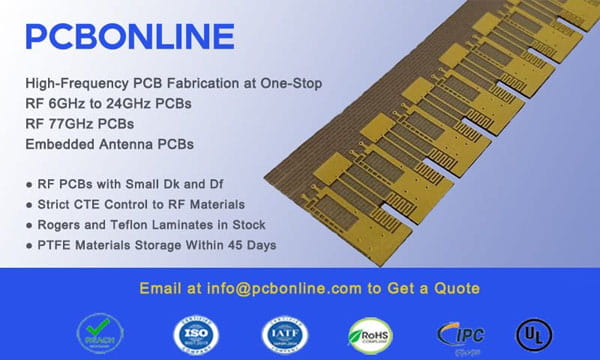
Designing a high-frequency PCB takes much time and energy, but if it works, all efforts are worth it! You can check if your high-frequency design works properly with the help of PCBONLINE. PCBONLINE, a one-stop high-frequency PCB manufacturer, provides you with free design for excellence. When you send your Gerber files to PCBONLINE, its engineers will check your high-frequency PCB design carefully. If there is something wrong with your design, they offer useful suggestions to help you improve it.
When PCBONLINE makes sure your high-frequency PCB is well-designed, you can have high-frequency PCB manufactured. PCBONLINE has these advantages in high-frequency PCB manufacturing:
- Make sure the impedance and line space are manufactured within the 2% tolerance range according to your high-frequency PCB design.
- Have ready-to-use high-frequency material in stock (storage period within 45 days) and turn your high-frequency PCB design into products quickly.
- Use the best high-frequency PCB materials of low Dk, Df, and water absorption (Rogers, Taconic, Arlon, etc.).
- Grasp the core technology in high-frequency PCB thermal expansion and contraction control.
- Have diverse high-frequency materials to choose from, such as PTFE, ceramics, FR4, ceramic-filled PTFE, ceramic filled with hydrocarbon, etc.
Online register and get $100 coupons for high-frequency PCB online purchases. You can contact PCBONLINE by email or online.
Conclusion
This article analyses the challenges in high-frequency PCB design of signal disturbance, and based on this, gives 11 useful design rules for high frequency. It also tells you how to check your design and have high-frequency PCBs manufactured. If you are looking for a one-stop solution, from PCB designing to the end products, send your idea to PCBONLINE, and you will receive satisfying results.


