

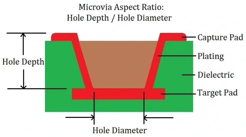
A microvia is a laser-drilled interconnect with an aperture of 150μm or less that connects two adjacent copper layers in an HDI PCB. Unlike a traditional through-hole via, which is mechanically drilled and passes through the entire PCB, a microvia only spans one layer pair. It matters when you are routing 2,000 connections out of a 0.4mm pitch BGA on a 24-layer PCB, as through-hole vias consume routing channels, while microvias free them up.
PCBONLINE manufactures HDI PCBs with laser microvias down to 0.075mm aperture for AI hardware, GPU PCBs, and high-speed computing systems. This article covers microvia structures, filling methods, and the manufacturing decisions that determine whether your PCB survives thermal cycling or fails.
Why Microvias Matter for AI and High-Speed Designs
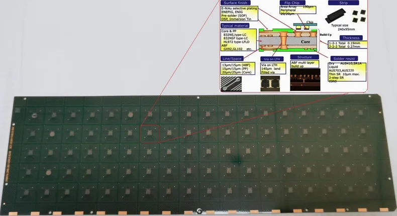
A GPU PCB or AI server PCB carries thousands of high-speed signal connections, dense power delivery networks, and components running at elevated temperatures. A standard through-hole via on a 0.2mm drill occupies space that could carry three or four fine-pitch traces. Multiplied across a PCB with hundreds of vias, you run out of routing space before finishing the BGA breakout.
Microvias create short vertical connections only between the layers that need them. The rest of the routing space stays open. Shorter electrical paths mean reduced parasitic capacitance and inductance, and better signal integrity for high-speed circuits running at 25+ Gbps.
For AI accelerators and high-performance computing hardware, the routing density difference between a standard multilayer PCB and an HDI PCB can determine whether a design routes cleanly or cannot be completed at all. Moving from a conventional stack-up to a 2+N+2 HDI structure can reduce PCB area by 30% while improving signal integrity margins.
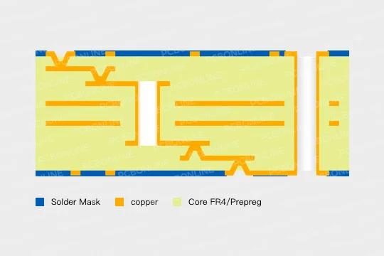
HDI Build-Up Structures: What 1+N+1 Through 4+N+4 Mean
HDI stack-ups are described by the number of build-up layers added on each side of the core. The "N" is the core layer count. The numbers on each side indicate how many sequential lamination cycles the PCB goes through.
1+N+1 HDI adds one build-up layer on top and one on the bottom of the core. This is entry-level HDI, with one laser drilling cycle and one sequential lamination. It works for compact consumer electronics and IoT devices where you need microvia escape routing but the layer count stays manageable.
2+N+2 and 3+N+3 HDI add multiple build-up layers on each side. Each additional build-up layer means another sequential lamination cycle, another round of laser drilling, and another round of copper plating. More build-up layers give more routing layers and higher component density, but each cycle adds manufacturing complexity and cost.
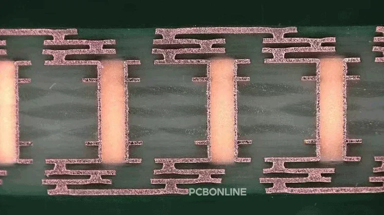
4+N+4 HDI is advanced. It requires four sequential lamination cycles on each side, precise microvia positioning across multiple layers, reliable via filling at every layer transition, and strict layer-to-layer registration control. This is what high-end AI hardware, GPU PCBs with 24+ layers, and fine-pitch BGA packages at 0.35mm pitch or below demand.
PCBONLINE supports HDI stack-ups from 1+N+1 up to 4+N+4, and any-layer interconnections, with up to 64 copper layers and impedance control within ±2%.
How Microvias Are Created: Drilling, Filling, and Plating
Understanding the manufacturing process helps you make better design decisions. Here is what happens after you submit your Gerber files and the PCB enters HDI production.
Laser drilling. A CO2 or UV laser ablates the dielectric material to create the microvia hole. The aperture typically ranges from 0.075mm to 0.15mm. At a 0.075 mm aperture, even a small registration error can shift the via off-pad and create a reliability problem.
Desmearing and seed layer. After drilling, the hole needs desmearing to remove resin residue left on the via walls by the laser. Electroless copper deposition then seeds the via walls with a thin copper layer.
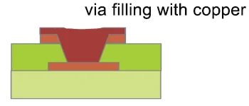
Electroplating and filling. Electroplating builds up the copper to create the electrical connection between layers. For stacked microvia structures, the via must be filled solid with copper rather than just plated on the walls. Copper filling creates a flat, conductive surface that the next build-up layer can laminate onto.
This is where most microvia reliability issues originate. If plating chemistry, current density, or filling speed is not properly controlled, voids form inside the via. Voids mean trapped air, and trapped air means thermal expansion stress that cracks the copper connection during reflow soldering or field operation.
Poor microvia filling shows up as copper cracks, connection failures during thermal cycling, and intermittent opens after assembly. For high-performance electronics operating under elevated temperature and high power, exactly the conditions an AI accelerator or GPU PCB faces, any of these failures are fatal and costly.
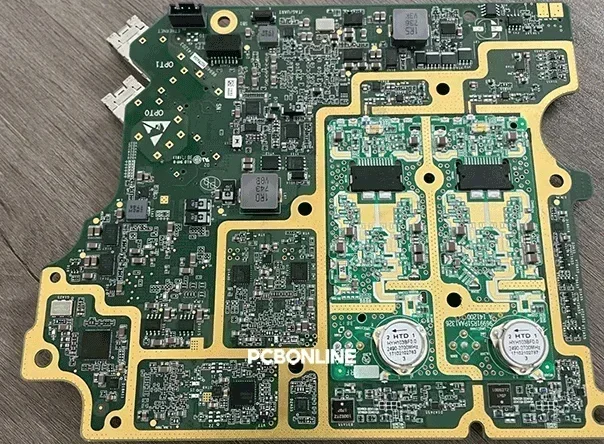
That's why OEM companies, solution companies, and product terminal companies choose PCBONLINE as their HDI PCB manufacturers for AI hardware and high-speed applications.
At PCBONLINE, microvia filling with copper/silver electroplating and with resin are also okay. Microvia filling with resin is not for electrical conductivity and is not a necessary step in the HDI manufacturing process. Its aim is to improve via-in-pad assembly reliability for BGA/CSP pads, which are common in HDI designs.
Stacked vs. Staggered Microvias

When your HDI structure requires microvias across multiple build-up layers to create a blind via, you have two structural options: stacked or staggered.
|
Factor
|
Stacked Microvias
|
Staggered Microvias
|
|
Structure
|
Vias placed directly above each other
|
Vias offset between layers
|
|
Routing density
|
Maximum; saves the most routing space
|
Moderate; uses slightly more area
|
|
Manufacturing difficulty
|
Higher; requires precise alignment and solid copper filling
|
Lower; more forgiving on alignment
|
|
Reliability risk
|
Higher; stacked vias carry more mechanical stress
|
Lower; stress distributed across different positions
|
|
Use case |
Advanced HDI, fine-pitch BGA escape, 4+N+4 structures
|
Moderate-density designs, cost-sensitive projects
|
|
Cost |
Higher
|
Lower
|
Stacked microvias are placed directly on top of each other, layer by layer. A via from Layer 1 to Layer 2 sits directly above a via from Layer 2 to Layer 3. This gives maximum routing density because the vertical connection path occupies the minimum XY footprint. The challenge is manufacturing precision: every via must align accurately with the one below it, and the copper filling must be void-free because stacked structures concentrate mechanical and thermal stress on the same vertical column.
Staggered microvias connect the same layers but at different XY positions. The via from Layer 1 to Layer 2 is offset from the via connecting Layer 2 to Layer 3. Alignment tolerance is more forgiving, and mechanical stress gets distributed across different positions rather than concentrated in one column. You give up some routing density, but gain production yield and reliability margin.
Stacked or staggered microvias? It depends on component density, layer count, signal requirements, and production volume.
For a prototype with a 0.4mm pitch BGA on a 2+N+2 structure, staggered microvias often provide enough density at lower risk.
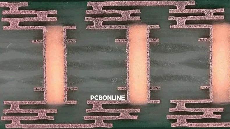
For a production AI accelerator PCB with 0.35mm pitch components on a 4+N+4 stack-up, stacked microvias may be the only way to achieve the required routing density.
This decision should happen during the DFM stage, not after the PCB is already in production.
Manufacturing Challenges You Should Know About
Three things cause the majority of HDI microvia failures in production.
Laser drilling accuracy. At a 0.075 mm aperture, the laser needs to hit a target pad that may be only 0.1mm wide. If the drill position drifts by 30μm, the via lands partially off-pad. The connection still forms during plating, but the reduced contact area creates a weak joint that fails under thermal stress. Layer-to-layer alignment tolerance becomes critical as build-up layers accumulate, because registration errors compound across each sequential lamination cycle.
Copper plating and filling quality. Plating bath chemistry, current density distribution, and filling speed all affect whether the via fills solid or traps a void. A void inside a single microvia may not cause an immediate electrical failure; instead, the connection tests fine on the bench. But under thermal cycling, trapped air expands and contracts, stressing the copper until it cracks. This is a latent defect that shows up in the application field.
Sequential lamination control. Each additional lamination cycle introduces the risk of layer misalignment, material deformation, and registration drift. A 4+N+4 structure goes through eight sequential lamination cycles total, with four on each side. If any cycle has a temperature or pressure deviation, the registration of all subsequent layers shifts. By the time you reach the final outer layers, accumulated error can push microvias off their target pads.
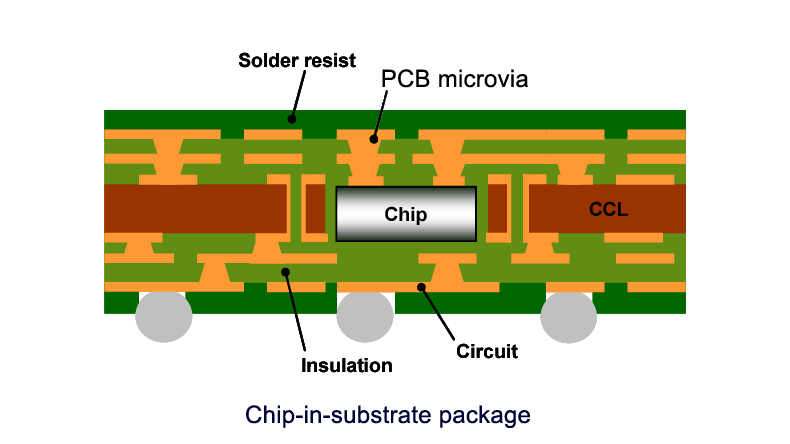
These are process control issues, not design issues. They do not show up in the Gerber files, but they determine whether the manufactured PCB is reliable. This is why the cheapest HDI quote is often the most expensive choice in the long run.
PCBONLINE, which aims to be a long-term manufacturing partner to help OEM and solution companies' products succeed, is the HDI manufacturer that you can rely on for quality.
How PCBONLINE Handles HDI Manufacturing
PCBONLINE provides complete HDI PCB manufacturing and assembly under one roof — engineering review, fabrication, component sourcing, SMT assembly, testing, and final delivery.

Founded in 2005, PCBONLINE has four locations for HDI manufacturing and assembly — two large advanced PCB manufacturing bases in Jiangsu and Jiangxi Provinces in China, one turnkey PCB assembly factory in Shenzhen, and a smart OEM center and headquarters also in Shenzhen.

Our HDI capabilities include stack-ups from 1+N+1 to 4+N+4, any-layer HDI, up to 64 copper layers, laser microvias down to 0.075mm, trace width/space control within ±0.02mm, and impedance control within ±2%.
Before any material is purchased, our engineering team performs a full DFM analysis covering microvia design, stack-up structure, trace width and spacing, impedance requirements, and manufacturing feasibility.
At our PCB assembly factory, PCBONLINE runs four fully automated SMT lines with 3D SPI, dual-stage 3D AOI, X-ray inspection for BGA and hidden-joint components, and first article inspection reporting on prototype orders.
Our combination of fine-pitch BGA assembly and X-ray inspection verifies both the microvia connections underneath the BGA and the BGA solder joints themselves.
Our experienced engineers provide one-on-one engineering support, solving technical and non-technical challenges while offering optimization suggestions to ensure your project runs smoothly from start to finish.
High-quality HDI PCB manufacturing certified with ISO 9001:2015, ISO 14001:2015, IATF 16949:2016, RoHS, REACH, UL, and IPC-A-600 Class 3.
Whether you need HDI PCB manufacturing and assembly to build AI servers, GPU boards, high-speed network equipment, or medical-grade systems, with 21 years of HDI PCBA manufacturing experience, we ensure that both electronics performance and final product presentation meet the highest standards. To get a quote for your HDI PCB project from prototype to bulk production, send your Gerber to info@pcbonline.com.
FAQ about HDI PCB Microvias
Q: What is the difference between a microvia and a through-hole via?A through-hole via is mechanically drilled and passes through the entire PCB, connecting all layers. It typically requires a 0.2mm or larger drill diameter. A microvia is laser-drilled with an aperture of 150μm or less and connects only two adjacent layers. Microvias free up routing space that through-hole vias would otherwise occupy.
Q: What does 2+N+2 mean in HDI PCB?It means two sequential build-up layers are added on each side of the core PCB. The "N" represents the core layer count. Each build-up layer requires its own laser drilling and sequential lamination cycle. Higher build-up numbers (3+N+3, 4+N+4) provide more routing layers but increase manufacturing complexity and cost.
Q: When should I choose stacked microvias over staggered microvias?Choose stacked microvias when you need maximum routing density for fine-pitch BGA escape routing on 3+N+3 or 4+N+4 structures. Choose staggered microvias when your design can tolerate slightly lower density but you want better manufacturing yield and reliability margin. The decision should be made during DFM review based on component pitch, layer count, and production volume.
Q: What causes microvia failures?The three most common causes are laser drilling misalignment (via lands partially off-pad), copper filling voids (trapped air that cracks the connection under thermal cycling), and sequential lamination registration errors (accumulated layer misalignment across multiple build-up cycles). All three are process control issues that do not show up in the design files but determine whether the manufactured PCB is reliable.
Q: Can PCBONLINE manufacture any-layer HDI PCBs?Yes. PCBONLINE supports any-layer HDI configurations with laser microvias down to 0.075mm, stack-ups up to 4+N+4, up to 64 copper layers, and impedance control within ±2%. The engineering team provides DFM review before production to validate microvia design and stack-up feasibility.
PCB assembly at PCBONLINE.pdf


