
As circuits are getting dense, PCBs (printed circuit boards) may require smaller holes to connect circuit traces in different layers. In a PCB design where space-saving is important, microvias are commonly used.
What is a microvia in PCB? This blog introduces microvias and reveals more details, including stacked microvias, stagger microvias, benefits of microvias, application of microvia PCBs, and microvia PCB manufacturer. Delving into the content below to know about PCB microvias!
In this article:
Part 1: PCB Microvia Part 2: Stacked Microvia Part 3: Staggered Microvia Part 4: Benefits of Microvia Part 5: Applications of Microvia PCB Part 6: One-Stop Microvia PCB Manufacturer PCBONLINEPCB Microvia
Microvia is a laser-drilled PCB via, with a diameter smaller than 6mil (0.1524mm). It is usually in the PCB outer layers and penetrates only one layer.
There are two ways to drill PCB holes or vias -- mechanical drilling and laser drilling.
Mechanical drilling drills multiple PCB layers at one time. The mechanical holes have a diameter of 0.15mm (6mil) and above. Mechanical drills can't create PCB holes smaller than 6mil or 0.15mm.
For microvias, the microvia PCB manufacturer PCBONLINE adopts laser drilling.
You may ask, why does a microvia penetrate only one PCB layer? Because the laser can penetrate fiberglass sheets but not copper. Besides, the fiberglass thickness should be within 0.13mm for the laser to penetrate.
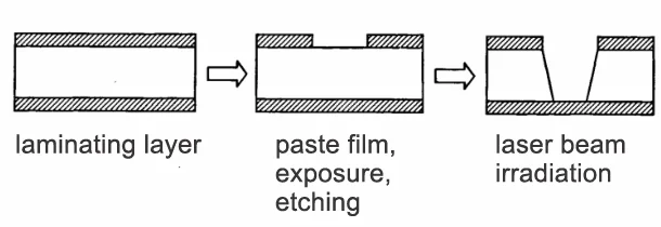
After laser drilling, the PCB manufacturer plates copper in the hole wall, and then a PCB microvia is formed.
The below figure shows the PCB microvia laser drilling process.
So here is the definition of PCB microvia -
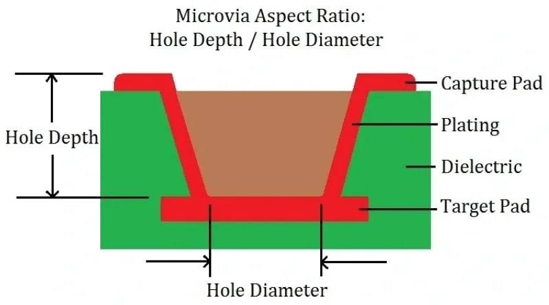
It is a laser-drilled hole smaller than 0.15mm that penetrates only one PCB layer, with a maximum aspect ratio of 1:1 (typically 0.75:1).
What is the aspect ratio of a microvia? It is expressed as:
Aspect ratio = Via Depth / Via diameter
The larger the aspect ratio, the more difficulty in microvia drilling, especially when the microvia diameter is minimal.
From the above knowledge, now you understand what a PCB microvia is.
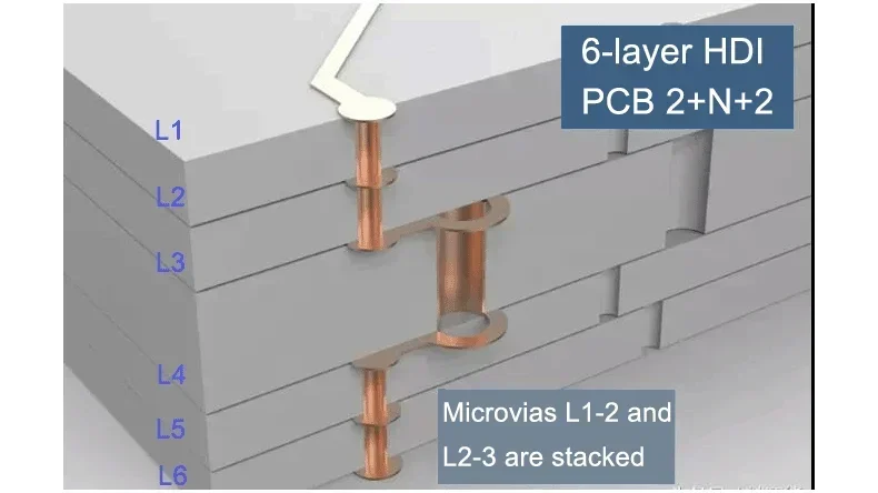
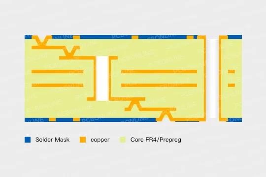
However, in an HDI (high-density-interconnect) PCB design, for example, the below 6-layer HDI PCB with a 2+N+2 stackup, you find that two microvias are stacked to form a hole in the outer layers. What is such a hole?
No worries. In the next parts, you will discover stacked microvias and staggered microvias!
Stacked Microvia
A stacked microvia is stacked by 2 or more layers of microvias.
In the above 2+N+2 PCB stackup, the two microvias in layer 1 and layer 2 form a stacked microvia (so is the case of layers 5-6).
This is how the stacked microvia is made in the above PCB stackup:
First, the PCB manufacturer finishes the PCB inner layers (the buried via in Layers 3-4 is a plated through hole that is mechanically drilled).
Second, the PCB manufacturer laser drills in Layers 2-3 and Layers 5-6.
Third, the PCB manufacturer plates copper that fills the microvias in Layers 2-3 and Layers 5-6.
Finally, the PCB manufacturer drills and plates microvias in Layers 1-2 and Layers 5-6 above the finished microvias in Layers 2-3 and Layers 4-5.
Now, the two microvias in Layers 1-3 and 4-6 form a stacked microvia separately.
At the PCB manufacturer PCBONLINE, you can have 1+N+1, 2+N+2, 3+N+3, and 4+N+4 stacked microvia PCBs manufactured and assembled.
Staggered Microvia
The below example explains what a staggered microvia is.
This 8-layer HDI PCB has a 2+4+2 stackup. In this stackup, the 2 means there are 2 layers of microvias in the outer layers separately at the top and bottom. The 2 microvias in Layers 1-3 are staggered and form a staggered microvia (so is the case of Layers 6-8).
Why are the 2 microvias staggered? Because copper plating does not fill the microvia, the PCB manufacturer cannot drill above it as the microvia is empty. Therefore, the PCB manufacturer has to drill the microvia in the other layer at a distance from it.
In the above PCB stackup, the 2 microvias at a distance are electrically connected and form a staggered via.
At the microvia PCB manufacturer PCBONLINE, a staggered microvia is composed of up to 4 microvias. That means, you can have 1+N+1, 2+N+2, 3+N+3, and 4+N+4 staggered microvia PCBs manufactured from PCBONLINE.
Stacked Microvia Vs Staggered Microvia
Here we make a comparison between stacked microvias and staggered microvias.
|
|
Stacked microvia
|
Staggered microvia
|
|
Microvia alignment
|
Yes
|
No
|
|
Copper filling via or not
|
Yes
|
No
|
|
Copper pad of the via
|
Closed
|
Open
|
|
Price
|
Higher
|
Lower
|
Note: The copper pad of a stacked microvia is closed because the via is filled with copper. A staggered microvia, on the opposite, has an open copper pad. In regards to why stacked microvias are more expensive, it is because of via filling plating and high-precision positioning in the fabrication process.
Benefits of Microvia
If your budget is enough for using a PCB whose microvias arbitrarily interconnect the PCB layers, you'll no longer be painstakingly in the PCB layout!
Besides allowing you to design a PCB with more autonomy, here are more reasons for you to consider using microvia in a PCB design:
Reduced parasitic capacity and inductance
Microvias have smaller diameters and depths and shorter signal paths than through holes. So using microvias in a PCB reduces the parasitic effect and improves the electrical performance.
Improved signal integrity and high-speed performance
Due to the microvia's smaller size and reduced parasitic effect, microvia PCB can transmit high-speed and high-frequency signals with minimal signal degradation and EMI (electromagnetic interference).
Affordability
Microvia PCBs can be very affordable! Imagine you want to design a multilayer PCB with 0.1mm diameter holes. If you make it a 1+N+1 stackup, the inner layers have a buried via with a 0.15mm-0.3mm diameter that is mechanically drilled, and the outermost layer in the top and bottom has a 0.1mm stacked microvia, you save a lot with such a microvia PCB design! Its price is even lower than a through-hole multilayer PCB.
Applications of Microvia PCB
As mentioned, microvias are commonly used in PCBs where miniaturization is a big deal, especially HDI PCBs. What about the applications of HDI PCB or microvia PCB? Here are their applications:
Smartphones and tablets
Many smartphones and tablets use 8-layer 1+N+1 microvia PCBs and 10-layer 2+N+2 microvia PCBs. iPhones even use arbitrarily interconnected microvia PCBs. By using microvia PCBs, smartphones and tablets feature high-resolution displays, powerful processors, etc, in a compact size with condensed circuitry.
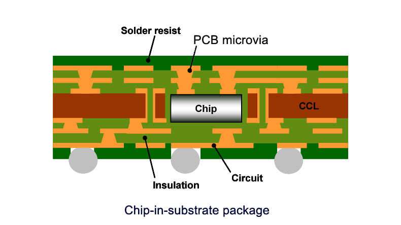
Microsystems
Microsystems is also called microelectromechanical systems (MEMS). Microsystem packaging such as CSP (chip-scale packaging), WLP (wafer-level packaging), and chip-in-substrate packaging use microvia PCBs. Besides, micropower systems and sensors use microvia PCBs.
Computers and peripherals
Microvia PCBs can be used in computer systems and peripherals, such as motherboards, graphic cards, memory modules, embedded systems, high-performance computing, etc.
Automotive electronics
Microvia PCBs find applications in automotive components and systems. Engine control units (ECUs), advanced driver assistance systems (ADAS), body control modules, and safety systems can use microvia PCBs in their design and manufacturing.
Wearable devices
You may find microvia PCBs in wearable electronics, for example, smartwatches, fitness trackers, and health monitoring devices. Microvia PCBs enable the integration of sensors, microcontrollers, wireless communication modules, and battery management circuits in these small devices.
Aerospace and defense electronics
As mentioned, micovia PCBs have good high-frequency signal integrity. Due to this, they can be used in avionics systems, communication systems, radar and sensor systems, and missile guidance.
Medical electronic devices
Microvia PCBs can even be used in medical electronics, such as gastroscopes, tiny therapy machines, and implantable devices can use microvia PCBs for high-density circuitry and compact space.
To sum up, microvia PCBs can be used in any application as long as keeping things small is crucial.
One-Stop Microvia PCB Manufacturer PCBONLINE
If you want to design advanced electronic products using microvia PCBs and have them manufactured, you can work with the HDI and microvia PCB manufacturer PCBONLINE.
PCBONLINE, founded in 1999, has two large advanced PCB manufacturing bases, one PCB assembly factory, and an R&D team to provide you with microvia PCB and embedding solutions.
PCBONLINE can meet your microvia PCB demands from the initial idea to high-volume production.
Minimum laser drill: 0.075mm, minimum mechanical drill: 0.15mm
We can make Microvia PCBs with structures of 100 µm and 125 µm.
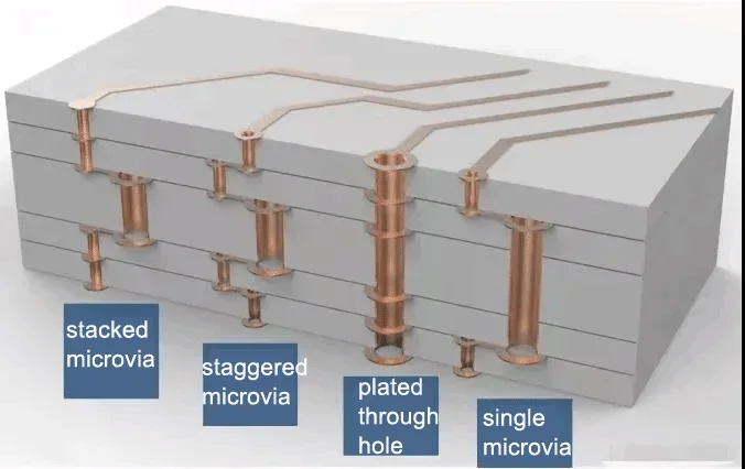
Microvias can be made as single microvias, staggered vias, stacked vias, and skipped vias.
High-density circuit layers up to 20, and microvia PCB layer up to 64.
Microvia PCBs 1+N+1, 2+N+2, 3+N+3, and 4+N+4 can be manufactured, and microvia can be in any layer in R&D.
PCBONLINE pays attention to quality and cost-effectiveness in HDI and microvia PCBs. Our engineers with more than 20 years of experience will provide you with one-on-one engineering support throughout the project. If you want to get a quote or ask questions, you can send emails to info@pcbonline.comto get a quote.
ConclusionThis article thoroughly demonstrates what a microvia is in PCBs, stacked microvias, staggered microvias, benefits, and applications. If you need micro via PCBs or have any doubts, you can contact PCBONLINE by email or from the table on the right.
PCB fabrication at PCBONLINE.pdf


