
AI servers, smartphones, aerospace applications, wearables, and industrial controls, due to the circuit complexity, 10-layer PCBs (printed circuit boards) are needed. A 10-layer PCB can be a high-Tg multilayer FR4 PCB, HDI (high-density-interconnect) PCB, rigid-flex PCB, or thick-copper PCB of 3oz+. Despite the different requirements of different applications, what is your 10-layer PCB choice?
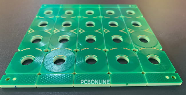
Choosing the right type of 10-layer PCB is critical for device performance and manufacturing cost-efficiency. At PCBONLINE, we manufacture and assemble all types of 10-layer PCBs, including FR4 multilayer PCBs, 10-layer HDI PCBs, 10-layer rigid-flex PCBs, and 10-layer thick-copper PCBs (3 oz copper and above). Our article explores the differences, stackups, and applications of 10-layer PCBs for your design considerations.
What Makes a 10-Layer PCB Necessary?
A 10-layer PCB consists of six signal layers and four plane layers (ground and power), though custom configurations can vary depending on EMI requirements. The transition from 8 layers to 10 layers is because of more shielding and tighter impedance control.

A 10-layer PCB is used because it provides:
- Superior EMI shielding: With 10 layers, designers can sandwich signal layers between solid ground planes, significantly reducing electromagnetic interference.
- High routing density and compact PCB side for complex ICs: For AI hardware, GPUs, FPGAs, and high-end CPUs have high pin counts. These BGA components require 10 or above layers to fan out. For AI servers and wearables, a PCB with 10 or above circuit layers enables them to perform many functions in a compact space.
- Thermal dissipation: Additional internal copper planes act as effective heat sinks for high-power components.
With a 10-layer PCB design, designers can achieve dedicated power and ground planes, RF or mixed-signal isolation, and high-speed digital signal integrity while using fine-pitch BGAs and SoCs. So 10-layer PCBs are necessary for AI servers, wearables, industrial controls, etc.
10-Layer Multilayer FR4 PCB
A 10-layer FR4 PCB uses glass-fiber–reinforced epoxy resin (FR4) as the base dielectric material and is fabricated through multiple lamination cycles. Due to the high number of layers and repeated thermal stress during lamination, high-Tg FR4 materials (Tg > 170℃) are used instead of standard FR4.
High-Tg materials provide improved dimensional control and prevent the PCB from warping or delaminating during the reflow soldering process and long-term operation. It ensures that the plated through-holes (PTH) maintain their integrity under thermal expansion.
10-layer high-Tg FR4 PCBs are used as high-end motherboards, including —
- Server motherboards, where multiple memory channels and PCIe lanes require extensive routing.
- Network switches handling massive data throughput with high signal integrity.
- Workstations and industrial computing platforms, supporting high-performance computing environments.
10-layer high-Tg FR4 PCBs feature conventional multilayer lamination, through-hole vias and buried vias, high-Tg FR4 materials, and a good balance of cost and performance.
10-Layer HDI PCB
When the pitch of your components below 0.2mm becomes too fine for standard mechanical drilling, HDI (High Density Interconnect) technology becomes essential. 10-layer HDI PCBs use microvias, laser drilling, and sequential lamination to achieve extreme density.
At PCBONLINE, the most common 10-layer HDI stackups are 2+6+2 and 3+4+3.
A 2+N+2 (2+6+2) stackup features two layers of laser-drilled microvias on the top and bottom, connected to a 6-layer conventional core. A 2+6+2 HDI PCB provides a high manufacturing yield and lower cost compared with deeper HDI structures. The 2+N+2 stackup is sufficient for most 0.4–0.5 mm pitch BGAs and is the most popular 10-layer HDI configuration.
Smartphone mainboards, AIoT SoC boards, compact embedded systems, and high-density consumer electronics use 2+6+2 10-layer HDI PCBs.
A 3+N+3 (3+4+3) stackup is more complex with three levels of sequential laser drilling, enabling faster signal breakout from ultra-fine-pitch BGAs. A 3+4+3 HDI PCB provides a superior fan-out capability and supports very small BGA pitch and high I/O count. However, it is more expensive and is used only when routing constraints cannot be solved with 2+6+2.
High-end smartphone SoC boards, advanced RF modules, and high-performance AI processors use 3+4+3 10-layer HDI PCBs.
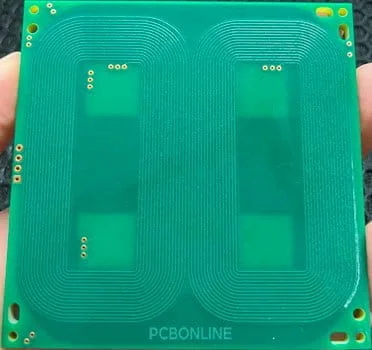
10-Layer Rigid-Flex PCB
A 10-layer rigid-flex PCB has a flexible PI (polyimide) FPC core of 2 or 4 layers.
Why 2 or 4 flex layers? The core advantage of rigid-flex PCBs lies in their flexibility. If the flexible PCB core has more than 6 layers, the FPC becomes thick, losing its flexibility and may even break the inner copper foil when bent. 2 or 4 layers of the FPC make the optimal balance between signal routing density and mechanical flexibility.
To prevent the 10-layer rigid-flex PCB from twisting during the high-temperature lamination, the flex layers must be centered. In the 10-layer rigid-flex PCB, the 2-layer FPC is placed at L5-L6 for signal layers, or a 4-layer FPC is placed at L4-L7 (L5-L6 for grounding and L4/L7 for signals).
A 10-layer rigid-flex PCB with a 2-layer FPC core maximizes the bend ratio. It is used for wearables and medical devices.
A 10-layer rigid-flex PCB with a 4-layer FPC core is used when signal density or EMI shielding is a priority, such as high-end smartphone camera modules or foldable devices where high-speed data (like MIPI CSI) must pass through the flex layers.
10-Layer Thick-Copper PCB
When your 10-layer PCB needs to carry high current, a thick-copper PCB with copper weights of 3oz or more is the solution.
Thick copper requires wide trace widths and large spacing because the chemical etching process for thick copper is aggressive. Therefore, 10-layer thick-copper PCBs prioritize power handling over routing density. If you need the 10-layer PCB to be thick copper, you must sacrifice the high density of HDI.
10-layer thick-copper PCBs are built for ruggedness and power and are used for:
- Industrial control systems, used in heavy machinery and motor drives, where high current and 10 layers of control logic must coexist.
- Aerospace power distribution systems, requiring extreme reliability and the ability to handle power surges in harsh environments.
- Automotive EV systems, especially battery management systems for electric vehicles, using 10-layer thick-copper designs for power routing.
Choosing the Right 10-Layer PCB Technology
When selecting a 10-layer PCB, designers should consider component pitch and I/O count, PCB size limitations, power and current requirements, mechanical constraints, and cost and manufacturing yield.
Here’s a quick comparison of the above 10-layer PCBs.
|
PCB type
|
Advantage
|
Application
|
|
10-Layer FR4
|
Cost-effective, stable
|
Motherboards, servers
|
|
10-Layer HDI
|
Extreme density
|
Smartphones, AIoT, RF, AI servers
|
|
10-Layer rigid-flex
|
Space optimization
|
Mobile, wearable devices
|
|
10-Layer thick-copper
|
High power handling
|
Industrial, aerospace
|
Here are design considerations for 10-layer PCBs.
Stackup symmetry — To prevent warping during the cooling phase of lamination, the 10-layer stackup must be symmetrical. This means that the materials and copper weights used on Layer 1 must match Layer 10, Layer 2 must match Layer 9, and so on.
Signal integrity and impedance — With 10 layers, you have enough ground planes. For high-speed designs (DDR4/DDR5 memory or PCIe Gen4/5), ensure that differential pairs are routed over a continuous reference plane to maintain 90-ohm or 100-ohm impedance.
Thermal management in thick copper — For 10-layer thick-copper PCBs, while the copper helps spread heat, the resin in the FR4 must be able to withstand the localized temperatures. Using high-conductivity thermal prepregs can assist in the 10-layer builds.
Partner with PCBONLINE for 10-Layer PCBs
If you need one-stop 10-layer FR4, rigid-flex, HDI, or heavy-copper PCB manufacturing and assembly, you can partner with PCBONLINE. PCBONLINE is an OEM PCB manufacturer that provides multilayer FR4 PCBs, heavy-copper PCBs, rigid-flex PCBs, HDI PCBs, and thermal-enhanced PCBs.

Founded in 2005, PCBONLINE has two large advanced PCB manufacturing bases, one PCB assembly factory, stable supply chains, and an R&D team for one-stop PCBA manufacturing.
PCBONLINE has strong PCB manufacturing capabilities, including FR4 PCB layers from 1 to 64, thick-copper PCBs up to 14oz, HDI PCBs, high-frequency PCBs, flexible PCBs, rigid-flex PCBs, aluminum PCBs, copper-based PCBs, and ceramic PCBs.
PCBONLINE grabs mature technologies for 10-layer PCBs, including controlled vacuum lamination for 10-layer rigid-flex and HDI structures, CO2 and UV laser drilling for 2+N+2 and 3+N+3 HDI configurations.
PCBONLINE offers free design for manufacturing (DFM) for your 10-layer PCB and PCBA project, including checking Gerber, bill of materials (BOM), testing files, and solving all technical and unexpected issues during prototyping to ensure the smooth and successful massive production.
PCBONLINE can do the R&D for your PCBA project or take part in your project's development from the early stage for the optimum PCB design and prevent tricky problems in the field application engineering (FAE) stage.
One-stop PCB services meeting your custom needs, including prototyping/sampling, PCB manufacturing, component sourcing, PCB assembly, PCBA value-added, testing, enclosure, and box-build assembly.
High-quality advanced PCB manufacturing certified with ISO 9001:2015, ISO 14001:2015, IATF 16949:2016, RoHS, REACH, UL, and IPC-A-600 Class 2/3.
No matter what applications your 10-layer PCB will be used for, like GPU AI servers, automotive, aerospace, medical devices, industrial controls, and consumer wearables, PCBONLINE can produce and assemble PCBs that meet the highest performance and reliability standards. To get a quote for your 10-layer PCB project, contact info@pcbonline.com.
Conclusion
A 10-layer PCB can be high-Tg FR4, rigid-flex, HDI, or thick-copper. Choosing the correct PCB structure depends on whether the priority is signal integrity, miniaturization, mechanical flexibility, or high current capacity. If you're designing a 10-layer PCB, PCBONLINE can provide one-stop PCB manufacturing for you with one-on-one engineering support.
PCB assembly at PCBONLINE.pdf
PCB fabrication at PCBONLINE.pdf


