
The formula P = V × R reminds us that power electronics must often deal with both high voltage and high current. While standard FR4 PCBs and flexible PCBs commonly operate in the 3.3V–24V range (3.3V, 5V, 12V being the most typical), many modern applications demand far higher voltages. High-voltage PCBs are essential for devices that operate at 100V to 1000V, or even higher.
High-voltage applications include industrial controls, industrial power supplies, inverters, EV charging piles, and specialized medical devices such as defibrillators. Building a PCB that can withstand such high voltages requires more than just thicker copper PCBs. High-voltage PCBs require wide trace space, high-voltage-withstand materials, high-voltage components, strict PCB quality control, and precise assembly.
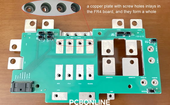
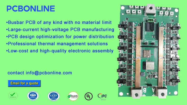
high-voltage PCB for EV charging pile
At PCBONLINE, we are not only a turnkey manufacturer but also an R&D-driven partner. With years of experience providing high-voltage PCB manufacturing and assembly, along with free DFM (Design for Manufacturability) checks, we help customers create safe, reliable, and high-performance solutions for demanding environments.
In this article, we'll explore what high-voltage PCBs are, essential design tips, manufacturing considerations, and why partnering with an experienced supplier like PCBONLINE makes all the difference.
Part 1. What are High-Voltage PCBs?
High-voltage PCBs are printed circuit boards designed to handle high voltage and high current loads. Unlike regular boards, they must manage strong electrical stress and significant thermal dissipation.
Standard PCBs' voltage range falls in 3.3V–24V (general electronics), while high-voltage PCBs handle from 100V to 1000V+ for industrial, automotive, and medical use.
Applications of high-voltage PCBs include:
- Industrial controls and automation systems
- High-voltage power supplies
- Inverters for renewable energy systems
- Electric vehicle (EV) charging piles
- Medical devices such as defibrillators
Common features of high-voltage PCBs are:
- Thick copper layers: Support high current and better heat dissipation.
- Large trace spacing: Prevents arc discharge and ensures safety at high voltages.
- Through-hole technology (THT): THT assembly is often required because through-hole components can withstand higher voltages compared to surface-mount devices.
- High thermal management needs: Heat must be dissipated efficiently to avoid component and system failure.
- Use of PCB busbars: Some high-voltage designs apply busbars for carrying large currents safely.
Besides, high-voltage PCBs can also be applied with a high-quality moisture-proof and dust-proof PCBA conformal coating. Conformal coatings effectively increase creepage distances and prevent surface leakage in high-humidity or polluted environments.
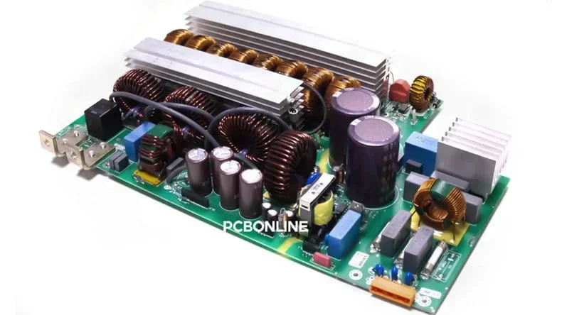
high-voltage PCB for the industrial inverter main board
Part 2. High-Voltage PCB Tips
Designing a reliable high-voltage PCB requires deep knowledge of electrical, thermal, and material behavior. At PCBONLINE, we combine our professional R&D capabilities with rich fabrication experience to help customers navigate these challenges. Below are our four high-voltage PCB design tips.
Tip 1: Designing PCB with Large Trace Space
The distance between copper traces is one of the most critical safety aspects of a high-voltage PCB. According to IPC-2221A, designers must calculate both:
- Electrical clearance: Shortest distance through the air between conductors.
- Creepage distance: Shortest distance along the PCB surface.
The required spacing is determined at the peak voltage, which equals the effective voltage multiplied by √2. Importantly, the spacing guidelines in IPC-2221A represent absolute minimums. In practice, adding a safety margin is recommended to prevent failures caused by environmental factors like humidity or contamination.
Below is a simplified IPC-2221A guideline table for minimum electrical clearance and creepage distance:
|
Peak Voltage (Vp)
|
Min. Electrical Clearance (mm)
|
Min. Creepage Distance (mm)
|
|
≤ 15
|
0.1
|
0.1
|
|
16 – 30
|
0.1
|
0.1
|
|
31 – 50
|
0.15
|
0.15
|
|
51 – 100
|
0.25
|
0.4
|
|
101 – 150
|
0.4
|
0.6
|
|
151 – 170
|
0.5
|
0.8
|
|
171 – 300
|
0.6
|
0.2
|
|
301 – 500
|
0.8
|
0.6
|
|
> 500
|
0.8 + 0.0025 × (V–500)
|
1.6 + 0.005 × (V–500)
|
Designers should always calculate based on peak voltage, compare both clearance and creepage values, and adopt the larger requirement with an added safety margin.
Tip 2: Using High-Voltage-Resistant PCB Materials
Material selection is another crucial factor. High-voltage PCBs need materials with a high CTI (Comparative Tracking Index), which measures resistance to electrical breakdown on the PCB surface.
High-Voltage PCB Insulation Material Table
|
Insulation Material
|
Typical CTI (V)
|
Thermal Conductivity (W/m·K)
|
Notes
|
|
High-CTI FR4
|
> 600
|
0.3 - 0.4
|
Industry standard, balancing cost and performance.
|
|
Polyimide (PI)
|
> 175
|
0.2 - 0.3
|
Used in high-temp and flexible applications.
|
|
Polytetrafluoroethylene (PTFE)
|
Excellent, no specific CTI value
|
0.2 - 0.3
|
Ideal for high-frequency applications; excellent dielectric properties.
|
|
Al2O3 (Alumina)
|
Excellent, no specific CTI value
|
20 - 35
|
High thermal conductivity ceramic substrate.
|
|
AlN (Aluminum Nitride)
|
Excellent, no specific CTI value
|
150 - 200
|
Extremely high thermal conductivity ceramic.
|
|
Si3N4 (Silicon Nitride)
|
Excellent, no specific CTI value
|
60 - 90
|
High strength and good thermal conductivity.
|
|
MCPCB Dielectric
|
> 600
|
1.0 - 9.0+
|
Specialized for high-power thermal management.
|
Tip 3: Using High-Voltage-Grade Components
Every component on the high-voltage PCB must be rated for the voltage environment.
Capacitors must have proper voltage grades, especially in power circuits.
Resistors must withstand higher voltages without overheating or drifting.
Connectors must have insulation and spacing that match high-voltage safety standards.
Choosing components that are voltage-grade certified prevents premature breakdowns and ensures compliance with safety regulations.
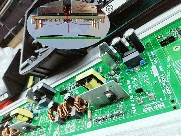
Tip 4: Anti-Arc PCB Design
Arc discharge is a serious failure risk in high-voltage systems. It often originates from sharp copper corners, where electric field concentration occurs. To prevent this:
- Use rounded corners on traces.
- Avoid acute angles in high-voltage areas.
- Maintain smooth copper edges for more even electric field distribution.
This anti-arc design significantly reduces the chance of unwanted discharge and extends PCB lifespan.
Part 3. High-Voltage PCB Manufacturing and Assembly
Manufacturing and assembling high-voltage PCBs presents challenges that go far beyond ordinary PCB production.
Through-Hole Technology (THT)
Since high-voltage PCBs rely heavily on THT components, PCB assembly requires specialized processes:
- Ensuring complete solder joint integrity and optimal solder volume is critical.
- Proper wave soldering techniques must be applied to avoid weak joints.
- Thermal management during soldering is more demanding due to thicker copper layers.
At PCBONLINE, we use custom wave soldering jigs to guarantee quality. We design the PCBA fixture for wave soldering to prevent long-leaded or lightweight components from lifting during soldering and ensure full solder fill for robust mechanical and electrical connections.
Thermal Dissipation and Copper Thickness
High-voltage PCBs are usually high-power PCBs as well, requiring
- Thicker copper layers (e.g., 2 oz, 3 oz, or more).
- Heat dissipation vias with strong copper plating to transfer heat effectively.
- Copper thickness inspection to confirm uniformity across the PCB.
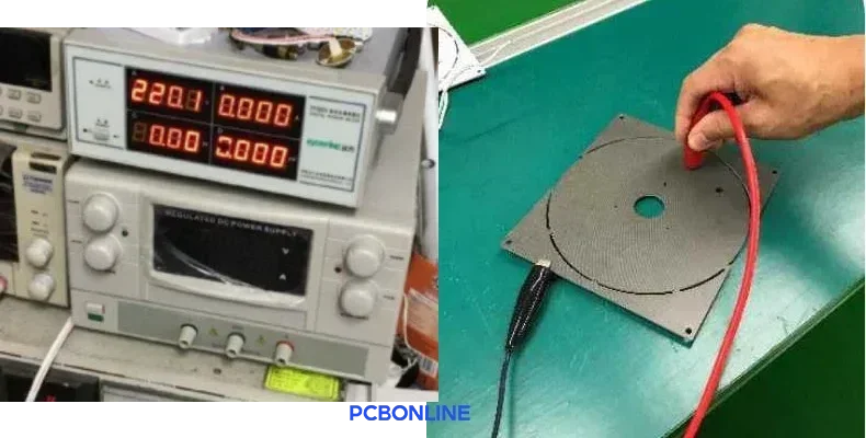
Hi-Pot Testing
Reliability testing is non-negotiable for high-voltage PCBs. PCBONLINE conducts Hi-Pot (High Potential) Tests, applying voltages significantly higher than the PCB's rated operating voltage to verify:
- No breakdown
- No leakage current
- Long-term operational safety
The high-pot test ensures the high-voltage PCB can handle its intended voltage stresses in real-world applications.
Part 4. Partner with PCBONLINE for High-Voltage PCBs
High-voltage PCB design, manufacturing, and assembly demand a level of expertise. That's why partnering with an experienced manufacturer, PCBONLINE, is essential.
Founded in 2005, PBONLINE has two large advanced PCB manufacturing bases and one PCB assembly factory. No matter what the expected voltage and power of the PCB are, PCBONLINE provides considerate manufacturing services with one-on-one engineering support throughout your project.
Available PCB substrate: FR4 of any Tg, ceramic, polyimide, polyester, PTFE (Teflon), aluminum, copper, and glass.
Copper thickness: any copper thickness in the range from 1/3oz to 14oz
Trace width/space: 1.6mil/1.6mil and above
PCB layers: FR4 PCB 1 to 64 layers, ceramic PCB and aluminum PCB 1 to 4 layers, copper base PCB 1 to 8 layers, flexible PCB 1 to 10 layers, rigid-flex PCB 2 to 30 layers, transparent flexible PCB 1 to 6 layers, high-frequency PCB and HDI PCB 4 to 24 layers, and glass PCB 1 layer
Quality certifications: ISO 9001:2015, IPC, IATF 16949, RoHS, REACH, and UL
PCB quantity: 1 to 100,000+
Lead time: 8 working hours to 4 weeks based on fabrication complexity
PCBONLINE will check your Gerber carefully to make sure your design is feasible and help solve technical issues. Besides, you can avail of PCB assembly, component sourcing, and value-added services such as conformal coating and box build assembly from PCBONLINE. If you feel interested in high-voltage PCB/PCBA from PCBONLINE, send your inquiry by email to info@pcbonline.com.
Conclusion
The large-voltage PCB design tips include increasing PCB trace space, using high-voltage-resistant material, using high-voltage-grade components, and anti-arc PCB design. If you need high-voltage PCB manufacturing and assembly, contact PCBONLINE to start your project with confidence.
©This article is an original work of the PCBONLINE team. Please indicate the author, PCBONLINE, if you reprint. If the article is reproduced without permission or without indicating the author's source, PCBONLINE reserves the right to investigate the infringement.
Battery Management System Manufacturing at PCBONLINE.pdf
CCS Product Introduction - PCBONLINE.pdf


