

Multilayer PCB assembly has the same process as single and double-layer PCB assembly. However, in production details, thermal management, and quality control, multilayer PCB assembly has more requirements.
Multilayer PCB Assembly Has More Thermal Requirements
Multilayer PCBs contain multiple internal layers of large-area copper foil for ground and power. So, a multilayer PCB assembly has more thermal requirements.
During reflow soldering, multilayer PCBs act like a heat sink, absorbing heat faster and in larger quantities. Achieving the required soak and peak temperatures during reflow requires more thermal energy than single/double-sided PCBs.
Multilayer PCB design should be as symmetrical as possible for even heating during PCB fabrication and assembly. If the PCB thickness or internal copper distribution is asymmetrical, surface pads may heat up too slowly, leading to cold solder joints or incomplete wetting.
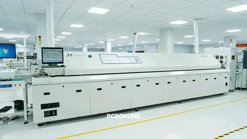
When reflowing and wave soldering multilayer PCBs, engineers from the PCBA manufacturer PCBONLINE usually extend the preheating time or fine-tune the oven's temperature profile to ensure internal and surface layers reach the melting point uniformly.
Warpage Control During Multilayer PCB Assembly
Multilayer PCBs accumulate internal stress during the lamination process in PCB fabrication. When exposed to high temperatures above 240°C, they are prone to warping if the stack-up design is not perfectly symmetrical.
Even slight deformation can cause solder joints on high-density components like BGAs or QFNs to bridge (short circuit) or stay open (no connection). Single/double-sided PCBs are much more structurally stable in this regard.
For standard multilayer PCBs' through-hole assembly, we control the warpage rate within 1.5%, and SMT assembly within 0.75%. If the multilayer PCB assembly requires high-precision SMT for BGA or QFN, we control the warpage within 0.5%.
For achieving the warpage control, the multilayer PCB design is as symmetrical as possible and uses high-Tg FR4 material. During PCB panelization in PCB design, V-cut depth is minimized, or instead, mouse bites are used to maintain a more rigid panel frame. Besides, we pay attention to the PCBA manufacturing process for warpage control.
During PCB assembly, we pre-bake PCBs that absorb moisture before SMT. The PCBs should be baked usually for at 120°C for 4 to 8 hours to remove moisture. Pre-baking prevents popcorning and internal stress caused by rapidly expanding steam during soldering.
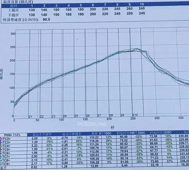
We also design a precise reflow profile with controlled cooling for the custom multilayer PCB assembly project. A gradual, controlled cooling rate of 2°C to 4°C per second allows the materials to settle more uniformly.
For thin PCBs under 1.0mm or large panels, using a synthetic stone or aluminum carrier/pallet provides a flat, rigid base that physically forces the PCB to remain flat throughout the heat cycle.
Vias and Pad Design of Multilayer PCBs
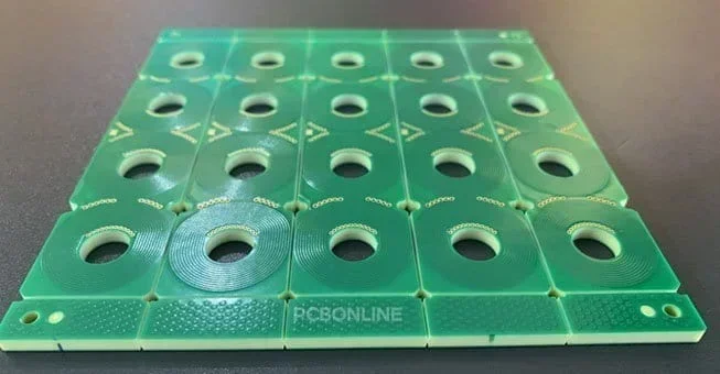
High-end multilayer PCBs often use blind or buried vias, called HDI PCBs. If these vias are near pads and the plugging process is poor, trapped air or residual solvents can expand during heating, leading to outgassing or solder balls.
Large components on multilayer PCBs often have thermal vias connected to internal copper planes. These pads dissipate heat so quickly that the solder paste may not melt properly without a specific thermal relief design or increased heat during SMT.
Here are the suggestions for via and pad designs of multilayer PCBs.
Via-in-pad technology
For high-density multilayer PCBs, especially with BGA pitches ≤ 0.8 mm, traditional "dog-bone" fanouts take up too much space.
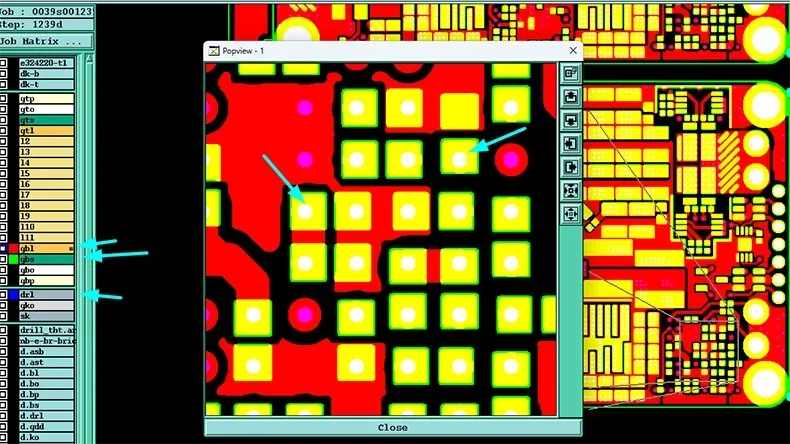
We suggest that the PCB design place the via directly inside the SMT pad. This saves routing space and reduces parasitic inductance.
The rule is never lto leave these vias open and specify IPC-4761 Type VII (Filled and Capped). The via is filled with non-conductive epoxy and plated over with copper to create a flat, solderable surface.
Thermal via design
Multilayer PCBs rely on internal planes to spread heat.
- Use an array like 3 × 3 or 4 × 4 of small vias under thermal pads of power ICs or MOSFETs.
- A via diameter of 0.3 mm is generally considered the "sweet spot" for thermal conductivity versus manufacturing cost.
- Keep a pitch of roughly 1.0 mm to 1.2 mm. If they are too close, they can weaken the board; if too far, they are ineffective.
- Ensure the vias connect to as many internal ground/power planes as possible to maximize the "heat sink" effect.
Annular ring & drill alignment
In multilayer PCBs, the drill must pass through many layers. If the drill "wanders" slightly, it can break the connection to an internal pad.
Follow IPC Class 2 (min 0.05 mm / 2 mil) or Class 3 (min 0.1 mm / 4 mil) standards.
Use "teardrop" shapes where a trace meets a pad or via. This adds extra copper at the junction, preventing open circuits if the drill is slightly misaligned.
Advanced via types for high density
Blind vias connect an outer layer to an inner layer, visible only from one side.
Buried vias connect internal layers only, not visible from the outside.
Staggered microvias offset from each other are more reliable and cheaper than stacked microvias that are placed directly on top of each other, which require more complex plating.
Pad design
Non-solder mask defined: The solder mask opening is larger than the copper pad. This is preferred for most SMT because it provides more surface area for the solder to "grip" the edges of the pad, resulting in a stronger joint.
Solder mask defined: The solder mask overlaps the copper pad. This is used for very fine-pitch BGAs to prevent the pads from lifting under thermal stress, though the solder joint itself is slightly smaller.
Partner with PCBONLINE for Multilayer PCB Assembly
If you need one-stop multilayer PCB manufacturing from prototyping to mass production, you can partner with PCBONLINE. PCBONLINE is an advanced PCB manufacturer that manufactures and assembles any type of multilayer PCBs, including multilayer FR4, HDI, flexible, ceramic, metal-core, and high-frequency.

Founded in 2005, PCBONLINE has two large advanced PCB manufacturing bases, one PCB assembly factory, stable supply chains, and an R&D team for one-stop PCBA manufacturing.
PCBONLINE has strong PCB manufacturing capabilities, including FR4 PCB layers from 1 to 64, high-density PCB, high-frequency PCBs, flexible PCB, rigid-flex PCB, aluminum PCB, copper-based PCB, and ceramic PCB.
PCBONLINE offers free design for manufacturing (DFM) for your PCB and PCBA project, including checking Gerber, bill of materials (BoM), testing files, and solving all technical and unexpected issues during prototyping to ensure the smooth and successful massive production.
PCBONLINE can do the R&D for your PCBA project or take part in your project's development from the early stage for the optimum PCB design and prevent tricky problems in the field application engineering (FAE) stage.
One-stop PCB services meeting your custom needs, including prototyping/sampling, PCB manufacturing, component sourcing, PCB assembly, PCBA value-added, enclosure, and box-build assembly.
High-quality advanced PCB manufacturing certified with ISO 9001:2015, ISO 14001:2015, IATF 16949:2016, RoHS, REACH, UL, and IPC-A-600 Class 2/3.
No matter what applications of your PCB are, like automotive, aerospace, medical devices, IoT, and high-end consumer electronics, PCBONLINE can produce and assemble PCBs that meet the highest performance and reliability standards. To get a quote for your PCB project, contact info@pcbonline.com.
Conclusion
The SMT and THT assembly processes for multilayer PCBs are the same as single and double-layer PCBs. However, multilayer PCB assembly has more requirements in soldering temperature control, warpage control, and via and pad design. PCBONLINE provides one-stop multilayer PCB manufacturing and assembly for mid and high-end applications. Send your Gerber to us or chat with us online for your project's multilayer PCB.
PCB assembly at PCBONLINE.pdf
PCB fabrication at PCBONLINE.pdf


