
As electronic devices and systems are getting smaller with more functions, the demands of multilayer printed circuit boards (PCBs) are higher. PCBONLINE, an OEM PCB manufacturer, offers all types of multilayer PCBs with higher circuit density and more compact forms.
Our article will help you understand what multilayer PCBs are, how they are made, and what types are offered at PCBONLINE (with layer counts and materials).
What is a Multilayer PCB?
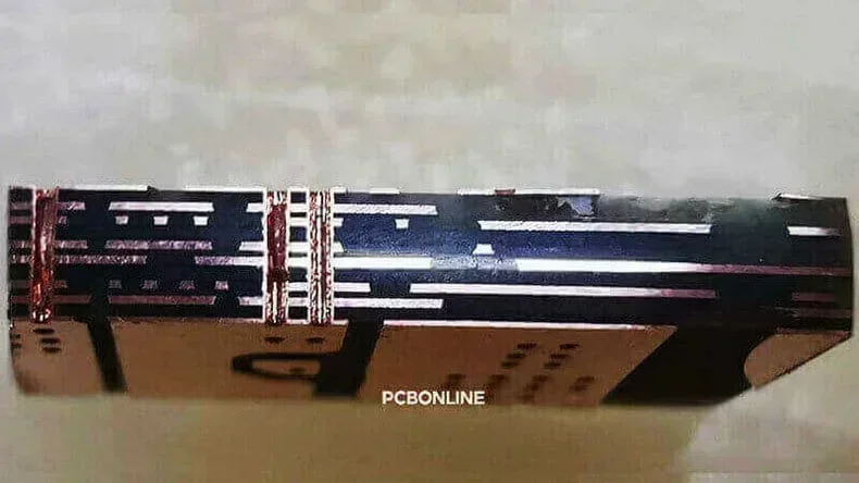
A multilayer PCB is a printed circuit board that has three or more copper layers. Multilayer PCBs begin at 3 layers and go up in complexity. The circuit layers are separated by insulating substrates (core material plus prepregs).
Multilayer PCBs allow:
- Higher wiring/circuit density in a smaller footprint.
- More flexibility in routing, especially for complex or high-speed systems.
- Improved electromagnetic interference (EMI) performance via dedicated ground and power planes.
- Better power distribution and signal integrity in high-frequency/high-performance applications.
Multilayer PCB Manufacturing Process at PCBONLINE
Here is a general workflow for how multilayer PCBs are fabricated at PCBONLINE (the process may vary depending on the layer count, type of material, HDI or not, etc.).
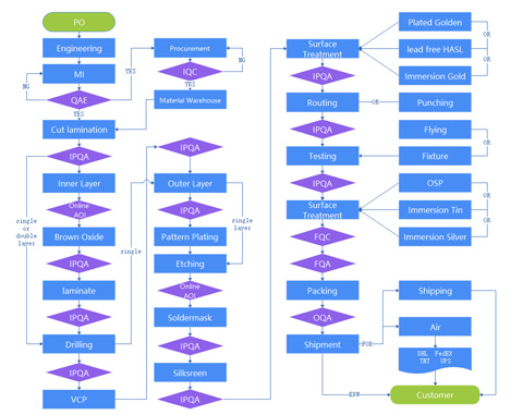
1. Material preparation / cutting the laminate
Selecting core materials, including FR4, flexible substrate, and PTFE, cutting cores, and preparing copper-clad laminates. Prepreg (pre-impregnated resin sheets) for interlayer bonding is also prepared.
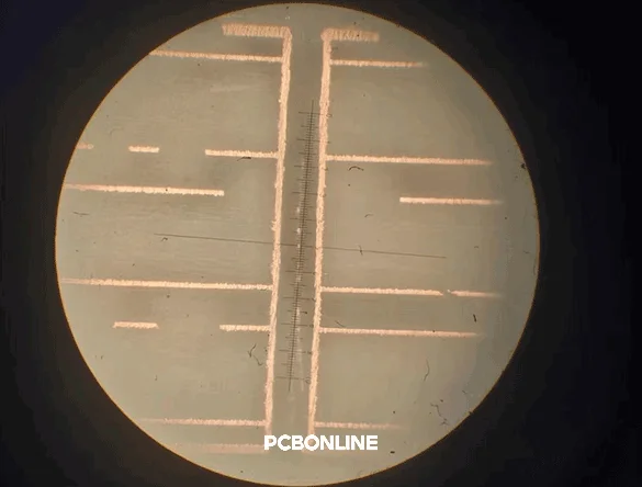
2. Inner layer imaging & etching
The inner copper layers are coated with photoresist, exposed via photolithographic masks/films, then developed and etched to remove unwanted copper. This forms the internal signal, power, or ground patterns.
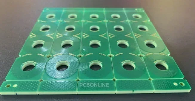
3. Lamination
The inner layers, prepreg, and core materials are stacked. High temperature and high pressure are applied to cure the resin in the prepreg, bonding the layers together without trapping air. For good adhesion, oxidation (e.g., brown oxide or black oxide) may be used on the copper surfaces to improve bonding.
4. Drilling and plated-through holes (PTH)
Once the laminate stack is formed, holes are mechanically drilled (PTH). For HDI (High Density Interconnect) multilayers, laser drilling or microvias may be done before or during lamination. After drilling, the hole walls are plated with copper to connect layers.
5. Outer layer imaging & etching
Outer copper layers (top & bottom) are patterned similarly via photoresist, exposure, development, and etching. Additional copper plating may be applied to circuit areas, followed by masking and removal of photoresist.
6. Solder mask, silkscreen & surface finishing
The PCB's copper surfaces (outside) are protected with solder mask. Silkscreen (legends, markings) applied. Surface finishes like ENIG (Electroless Nickel Immersion Gold), HASL, OSP, immersion tin/silver, etc., are applied to pads/contacts.
Profiling/routing/panelization
The PCBs are cut from panels, edges treated (e.g., routed, scored, V-cut). Any features like half-holes, slots, etc., are made.
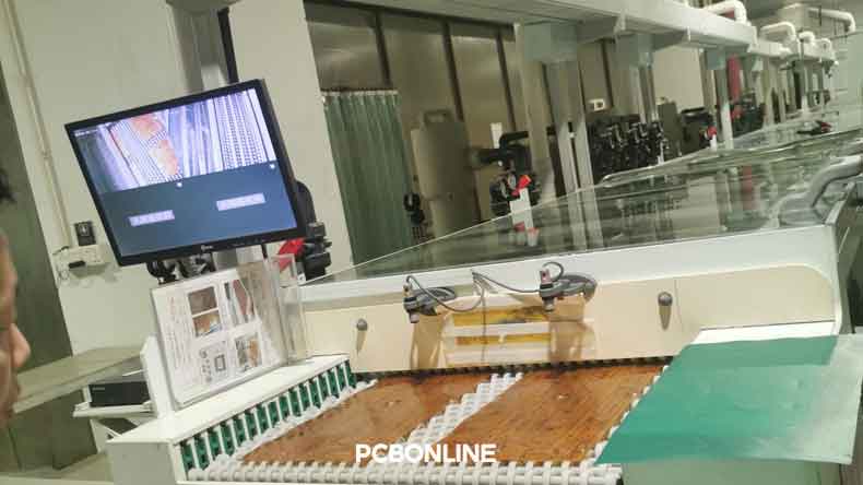
8. Inspection & testing
Automatic optical inspection (AOI), electrical testing (e.g., flying probe or bed-of-nails), and sometimes four-terminal sensing for critical boards (medical, automotive, aerospace). Final quality control before packaging.
9. Packaging & shipping
Once quality is assured, PCBs are cleaned, packaged appropriately for protection, and shipped (PCBONLINE offers a variety of freight methods: air, sea, rail via carriers like DHL, FedEx, UPS).
For multilayer PCB types like HDI, flex, and rigid flex, there are additional or modified steps (microvia formation, flexible substrate treatments, bending tests, etc.
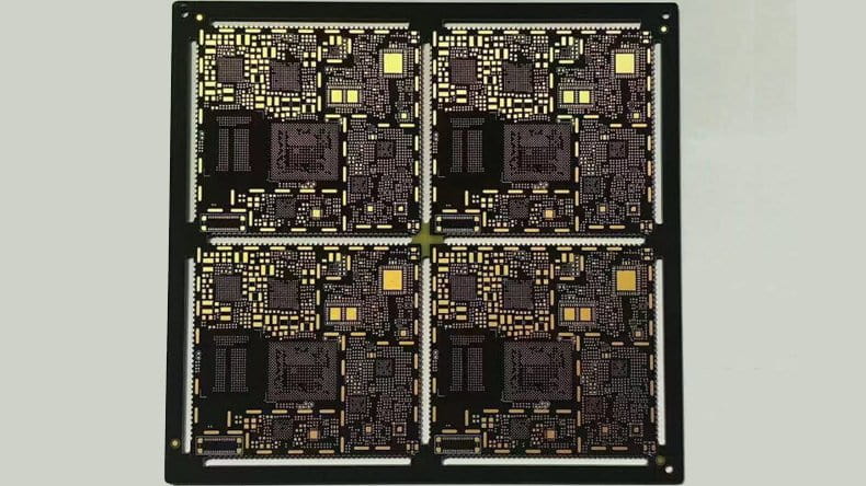
Types of Multilayer PCBs Offered at PCBONLINE
PCBONLINE offers multiple types of multilayer PCBs to suit different application needs. Below is an overview of our major types, typical layer counts, materials, and when each is used.
|
Type
|
Layer count range
|
Key materials/substrates
|
Applications/advantages
|
|
FR4 multilayer PCB
|
4 to 64 layers
|
Standard FR4, High-TG FR4 material for thermal stability
|
General electronics, computers, communications, power distribution, and large-volume PCBs where cost vs performance balance matters.
|
|
HDI PCB
|
4 to 64 layers with microvias / laser drilled
|
FR4 substrate, fine copper foils, laser drilling
|
Mobile devices, compact electronics, RF / high speed, and aerospace, where routing density and signal integrity are critical.
|
|
2 to 6 layers or in some cases up to 8
|
Flexible dielectric (polyimide or polyester), flexible copper foils, adhesives, or flexible prepregs.
|
Wearables, foldable devices, dynamic flexing parts, and medical devices where mechanical flexibility matters.
|
|
|
Rigid-flex PCB
|
2 to 24 layers
|
FR4 and polyimide substrate
|
Space-constrained designs, aerospace, military, medical implants, devices with moving hinges or folding parts.
|
|
High-frequency PCB
|
4 to 24 layers
|
PTFE, Rogers, ceramics, specially formulated FR4 / laminates, or Rogers/FR4 hybrid laminates, good dielectric constant control, strict impedance control.
|
High-speed digital, RF, and microwave systems, antennas, and high-frequency communication gear.
|
Layer Count and Stack up
PCBONLINE can fabricate multilayer PCBs with up to 60 or 64 layers, especially for FR4 materials.
- For rigid-flex PCBs, the layer count usually falls within 2 to 24 layers.
- Flexible multilayer PCBs are more limited due to mechanical constraints, commonly up to 8 layers in certain designs.
- High-frequency multilayer PCBs also stay in the 4-24 layer range to balance performance, cost, and manufacturability.
ceramic PCBs made by PCBONLINE
Stack-ups involve careful assignment of signal, ground, and power planes. For example, in a 6-layer FR4 PCB, you might have.
Top signal / ground / signal / signal / power / bottom signal
Or variations balancing GND, power, and signals for controlled impedance and EMI reduction.
Multilayer PCB Design & Manufacturing Considerations
Symmetry in layer structure is important to reduce warpage during lamination. When planning a multilayer PCB, there are other considerations.
1. Material selection
Choosing substrate (FR4 vs high-TG FR4 vs Rogers/PTFE vs flexible materials) will affect thermal performance, signal integrity, dielectric losses, cost, and mechanical stability.
2. Layer count vs cost & yield
More circuit layers often mean more complexity, risk of defects, and higher cost. Manufacturers like PCBONLINE have capabilities up to 64 layers, but for many designs, fewer layers of 4-16 often suffice. Use extra layers only when routing, isolation, and power-plane demand it.
3. HDI & via technologies
For high-density or compact designs, microvias, blind/buried vias, laser drilling, etc., are required. These add cost and require precise process control.
4. Stackup & impedance control
For high-speed or RF circuits, proper placement of ground/power layers, maintaining dielectric thickness, trace width/spacing, and controlled impedance are essential.
5. Thermal management
Heat dissipation paths (thermal vias, copper pours), materials with good thermal conductivity, and sometimes metal cores. Surface finish can also affect thermal behavior.
6. Surface finish & regulatory/environmental specs
Finishes like ENIG, HASL, OSP, immersion tin/silver, RoHS, REACH, UL, IPC certification. PCBONLINE holds ISO 9001, IATF 16949, RoHS, REACH, UL, and IPC certifications.
7. Quality & inspection
Methods such as AOI, electrical testing (flying probe, bed-of-nails), and four-terminal sensing are used when needed. PCBONLINE describes final QC, packaging, etc.
8. DFM / engineering support
Early design review helps avoid costly mistakes (minimum trace widths, via reliability, panelization, warpage). PCBONLINE offers free Design for Manufacturing (DFM), Design for Test (DFT), etc.
To get the best results when ordering a multilayer PCB from PCBONLINE, consider the following:
- Prepare your Gerber / IPC-2581 / ODB++ files carefully — ensure all layers (copper, solder mask, silkscreen, drill) are correct.
- Specify stack up early — decide how many ground/power planes, signal layers you need, and ensure symmetry
- Consider HDI if needed — if you need very fine features, blind/buried vias, microvias, make sure to inform during design.
- Choose material appropriate to the environment — thermal, mechanical, frequency demands.
- Specify surface finish and other process requirements clearly (e.g., ENIG, HASL, OSP, copper thickness, minimum trace/space, etc.).
- Check for DFM feedback — welcome any design suggestions from PCBONLINE's engineering team.
- Plan for testing & qualification — especially for critical industries (automotive, medical, aerospace). Use required inspection and test methods (AOI, flying probe, four-terminal sensing, etc.).
- Allow for tolerances — manufacturing tolerances in layer alignment, copper thickness, etc. Be realistic in spec.
4-, 6-, and 8-layer PCBs
The 4-layer PCB manufacturing process starts with the inner two layers, then lamination, drilling, outer layer patterning, solder mask, finish, silkscreen, testing, etc. The PCB may include "1+2+1" HDI variants (one outer, two inner, one outer) for a special design.
For 6-layer PCBs, the structure involves a core plus layers on both sides. Typical stackups include combinations of signal layers, ground, and power planes. Manufacturing involves more complex lamination, more drilling/plating steps.
8-layer PCBs are used where higher reliability and performance are needed. These involve more complex material selection, tight control of layer-to-layer alignment, signal integrity, and thermal management. PCBONLINE's guide shows best practices in design, manufacturing steps, and tips for handling such PCBs.
Order Multilayer PCB Manufacturing Services from PCBONLINE
If you need one-stop multilayer PCB manufacturing from prototyping to mass production, you can partner with PCBONLINE. PCBONLINE is an advanced PCB manufacturer that manufactures and assembles any type of multilayer PCBs, including multilayer FR4, HDI, flexible, ceramic, metal-core, and high-frequency.

Founded in 2005, PCBONLINE has two large advanced PCB manufacturing bases, one PCB assembly factory, stable supply chains, and an R&D team for one-stop PCBA manufacturing.
PCBONLINE has strong PCB manufacturing capabilities, including FR4 PCB layers from 1 to 64, high-density PCB, high-frequency PCBs, flexible PCB, rigid-flex PCB, aluminum PCB, copper-based PCB, and ceramic PCB.
PCBONLINE offers free design for manufacturing (DFM) for your PCB and PCBA project, including checking Gerber, bill of materials (BOM), testing files, and solving all technical and unexpected issues during prototyping to ensure the smooth and successful massive production.
PCBONLINE can do the R&D for your PCBA project or take part in your project's development from the early stage for the optimum PCB design and prevent tricky problems in the field application engineering (FAE) stage.
One-stop PCB services meeting your custom needs, including prototyping/sampling, PCB manufacturing, component sourcing, PCB assembly, PCBA value-added, enclosure, and box-build assembly.
High-quality advanced PCB manufacturing certified with ISO 9001:2015, ISO 14001:2015, IATF 16949:2016, RoHS, REACH, UL, and IPC-A-600 Class 2/3.
No matter what applications of your PCB are, like automotive, aerospace, medical devices, IoT, and high-end consumer electronics, PCBONLINE can produce and assemble PCBs that meet the highest performance and reliability standards. To get a quote for your PCB project, contact info@pcbonline.com.
Conclusion
Whether a 4-layer FR4 PCB, a 24-layer rigid flex, or a high-frequency PCB, it is a multilayer PCB. If you're designing a multilayer PCB, PCBONLINE can provide one-stop manufacturing for you.
PCB assembly at PCBONLINE.pdf
PCB fabrication at PCBONLINE.pdf


