
In surface mount technology (SMT), reflow soldering is a process that melts solder paste to permanently attach electronic components to printed circuit boards (PCBs). A proper reflow soldering process ensures electronics product quality and reliability.
PCBONLINE is an OEM PCB assembly manufacturer with reliable reflow soldering. This guide explains what reflow soldering is and its process, reflow profile, design considerations, such as PCB edge rails, and advanced reflow methods, including nitrogen reflow and vacuum reflow, and also inspections before and after reflow.
What is Reflow Soldering?
Reflow soldering uses hot winds to melt solder paste to solder surface-mount components (SMDs) onto a PCB.
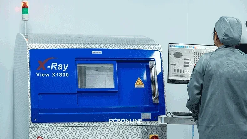
During SMT assembly at PCBONLINE, a solder paste printer applies solder paste onto PCB pads, an SPI machine inspects the solder, three pick-and-place machines place SMDs onto the solder paste, an AOI machine inspects the component placement, the assembly passes through a reflow oven with controlled heating, and then the second AOI machine inspects the soldering quality. Hidden joints additionally require an X-ray inspection.
When passing the reflow oven, the solder paste melts, and at the peak, with the PCB surface finish and SMD leads, it forms a strong metallurgical bond between SMDs and PCB pads. Once cooled, the solder joints harden, securing the components permanently.
Reflow soldering is a widely used soldering method in electronics assembly because it is:
- Repeatable and automated
- Capable of handling fine-pitch devices (01005, 0201, 0402, BGA, CSP, QFN)
- Compatible with prototype and large-scale production
- Reliable in creating consistent solder joints
The Reflow Soldering Process
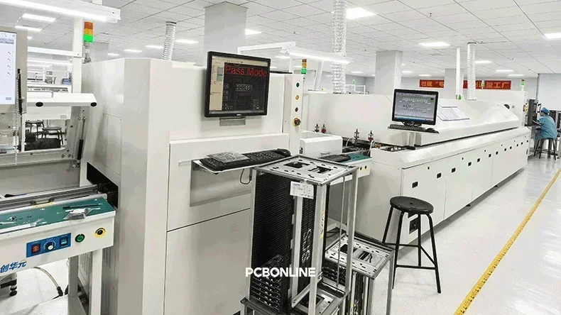
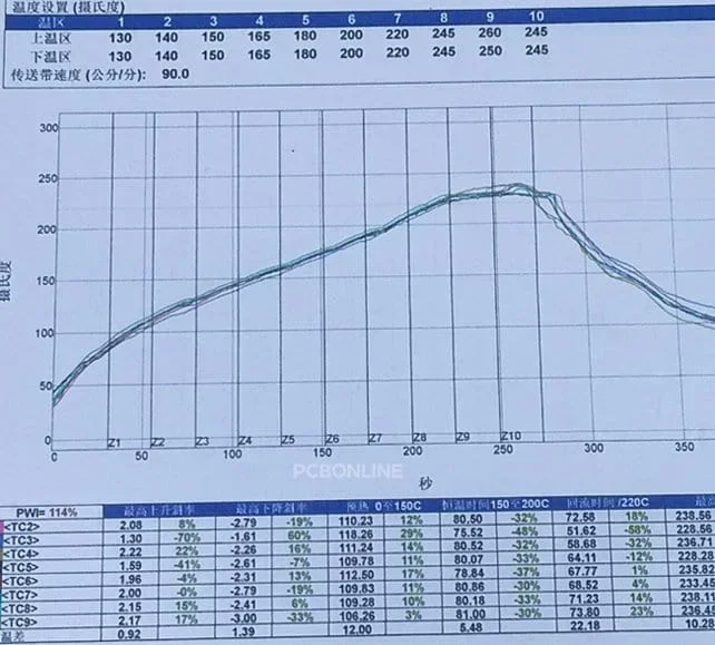
PCBONLINE's reflow ovens have 10 temperature zones, and the reflow soldering process is programmable following the reflow profile designed by our engineers.
A reflow profile defines how temperature changes inside the oven. It ensures solder paste activation, melting, and cooling happen correctly without damaging components.
A typical reflow profile includes four main stages:
1. Preheat (ramp-up)
The PCB is gradually heated to avoid thermal shock. Flux activation begins in this stage.
2. Soak (thermal equilibrium)
For every prototype circuit board assembly project, we also open a solder paste stencil for SMT assembly.
3. Reflow (peak zone)
Temperatures are stabilized to ensure uniform heating across the PCB. This reduces voids and eliminates solder spattering.
4. Cooling
Controlled cooling solidifies the solder. Too rapid cooling can cause thermal stress, while too slow cooling can form weak joints.
Preheat, soak, and reflow are reflow heating. Temperature changes in heating and cooling must be carefully controlled to avoid defects such as solder bridging, tombstoning, or component cracking.
Typical reflow profile settings are in the table below.
|
Stage
|
Temperature range (°C)
|
Duration
|
Purpose
|
|
Preheat ramp
|
25 - 150
|
60–120 sec
|
Avoid thermal shock, activate flux
|
|
at least 7/12mil
|
150 - 180
|
60–120 sec
|
Even heat distribution
|
|
2oz
|
245 - 250 (lead-free)
|
20–40 sec
|
Solder paste melts and wets pads
|
|
at least 7/12mil
|
250 - 180
|
30–60 sec
|
Solidify solder joints
|
Note: Exact settings depend on the PCB requirements. If it is a PI flexible PCB and FR4 PCB, the peak temperatures are 245°C to 250°C, while a PET flexible PCB is 130°C to 160 °C, and a thick-copper PCB is 260°C to 280°C.
PCB Design Considerations for Reflow Soldering
Reflow soldering success is not only about the reflow profile. Proper PCB design plays a major role in achieving reliable soldering, including edge rails, SMT stencil design, and component orientation.
1. Edge rails for PCB clamping
During reflow, PCBs are transported through ovens using conveyor rails or clamping mechanisms. To avoid interfering with solder pads or components, designers must leave edge rails (or handling strips) on both sides of the PCB.
- Standard clearance: 3mm to 5mm on each edge
- No copper traces, vias, or components should be placed in this zone
- Edge rails are later removed by depanelization
Without proper edge rails, PCBs can misalign or damage components during reflow.
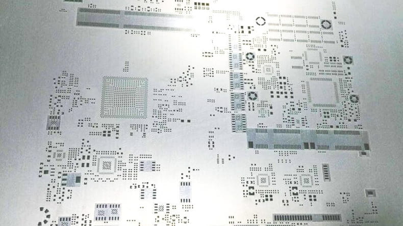
2. SMT stencil design
The solder paste stencil must match the pad dimensions precisely. Don't worry, SMT stencil design is not your job, as PCBONLINE includes it in our free design for manufacturing (DFM). We have rich experience in SMT stencil design. Our stencil tips are:
- Fine-pitch ICs and QFPs – To minimize stress concentration, we design the aperture ends with rounded corners.
- BGAs and ultra-miniature passives (0402, 0201) – Square apertures are applied to achieve uniform solder ball formation.
- QFN ground pads – A cross-shaped ("+") aperture pattern is used, keeping at least 0.5 mm clearance from the pad edge to prevent solder beading and to ensure effective grounding.
- USB, Mini USB, and CF/SD connectors – For grounding apertures, the length is extended at a 1:1.2 ratio to increase solder volume. An inward concave opening is adopted to reduce stress and suppress solder bead formation.
- General BGA aperture guideline – The aperture width should be sufficient for at least four solder balls to pass through, ensuring stable reflow performance.
3. Component orientation
Long-shaped components such as capacitors, inductors, connectors, and headers should be placed perpendicular to the conveyor direction. This prevents hot air flow inside the reflow oven from lifting or tombstoning the components, and ensures uniform soldering quality.
Advanced Reflow Methods
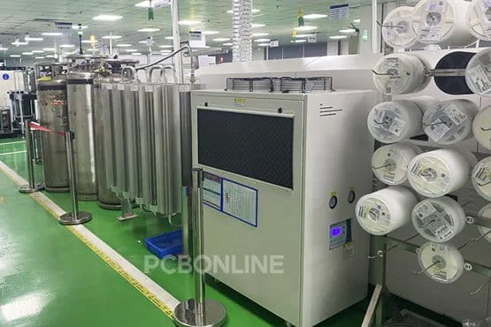
Standard reflow ovens use ambient air, but oxygen may cause oxidation of solder joints for sensitive components. For this, PCBONLINE also provides two advanced reflow soldering options: nitrogen and vacuum reflow soldering.
Nitrogen reflow soldering
Nitrogen reflow soldering introduces nitrogen gas into the oven, reducing oxidation and improving solder joint quality. It is beneficial for:
- Fine-pitch BGAs and CSPs
- High-reliability applications (automotive, aerospace, medical)
- Reducing solder voids and wetting issues
Vacuum reflow soldering
Vacuum reflow soldering is an advanced method that applies a vacuum during the peak soldering stage. By reducing the chamber pressure while the solder is molten, trapped gases inside the solder are eliminated, significantly lowering solder voids.
- Minimized void formation in solder joints, especially for BGAs, QFNs, and power devices.
- Improved thermal and electrical conductivity by ensuring nearly void-free connections.
- Enhanced reliability for high-power and high-frequency applications where heat dissipation is critical.
Inspection Before and After Reflow
How to check the quality of reflow soldering? Visual inspections are not enough. We use pre- and pro-reflow AOI inspections. For hidden joints, we also use the X-ray.
- AOI before reflow: It ensures correct solder paste printing and component placement.
- AOI after reflow: It checks solder joint quality, alignment, and polarity.
- X-Ray Inspection: For hidden solder joints (such as BGAs, CSPs, and QFNs), X-ray inspection is essential to detect voids, bridging, or insufficient wetting.
Our dual-AOI and X-ray inspections further minimize rework risks and ensure long-term product reliability.
Common Reflow Defects
What are the defects resulting from poor reflow soldering? They are:
- Tombstoning – Caused by uneven solder paste melting, pulling small components upright.
- Bridging – Excess paste or poor stencil design leads to shorts.
- Voids – Trapped gases create gaps in solder joints.
- Head-in-pillow – In BGAs, incomplete wetting causes poor contact.
PCBONLINE ensures these reflow defects won't happen to the PCBAs we deliver to you. We can adjust stencil design, optimize reflow profiles, use nitrogen reflow, and perform 100% functional PCBA and aging (burn-in) testing to prevent them.
Partner with PCBONLINE for PCB Assembly with Reliable Reflow Soldering
Whether you are designing for consumer electronics, automotive systems, or industrial IoT devices, you can partner with PCBONLINE for one-stop PCB assembly with high reliability. We provide SMT assembly, PTH assembly, PCB fabrication, component sourcing, fixtures, enclosures, box-build assembly, value-added services, testing, and shipping the finished devices you can sell.
PCBONLINE is an OEM PCBA source factory manufacturer founded in 2005. It has two large advanced PCB manufacturing bases independently fabricating all types of PCBs, one EMS (electronic manufacturing service) PCB assembly factory with two component warehouses, stable supply chains, and an R&D team. Besides, it keeps long-term cooperation with the top 3 mold/enclosure manufacturers in China to provide the molds, jigs, and enclosures for full box-build solutions.
Our PCB assembly, including reflow soldering, supports complex PCBs like HDI and flexible assemblies, with 100% X-ray inspection of hidden joints and 3D AOI testing.
Each SMT line at PCBONLINE is equipped with three advanced pick-and-place machines, supporting up to 376 SMD placements per PCB, enabling us to handle all types of SMT assembly, including high-density and large-format PCBs.
Our engineers have rich experience in reflow temperature control, and our reflow ovens are lead-free with 10 temperature zones.
We conduct first-article inspections both before prototype assembly and before mass production to ensure the highest PCBA quality and prevent costly issues.
By BOM component sourcing and in-stock warehousing, as well as PCB optimization advice, we reduce the circuit board assembly costs without quality sacrifice.
Our experienced R&D and engineering teams provide one-on-one support, solving technical and non-technical challenges while offering optimization suggestions to ensure your project runs smoothly from start to finish.
High-quality PCBA manufacturing certified with ISO 9001:2015, ISO 14001:2015, IATF 16949:2016, RoHS, REACH, UL, and IPC-A-610 Class 2/3.
When your project enters the bulky production stage, PCBONLINE refunds the fees of prototyping, including its value-added services.
Whether you need 10 prototype circuit board assemblies or 10,000 production units, PCBONLINE ensures that every PCBA meets the highest reliability standards. To get a quote from the SMT PCBA manufacturer PCBONLINE, contact info@pcbonline.com.
Conclusion
Reflow soldering requires properly setting the right reflow profile, designing PCB edge rails and an SMT stencil, and using AOI and X-ray inspections. With rich experience in temperature control and SMT soldering, we provide professional reflow soldering and SMT assembly services. To ensure the success of your PCBA projects, send the quote request from the table on the right to work with PCBONLINE.
PCB assembly at PCBONLINE.pdf


