
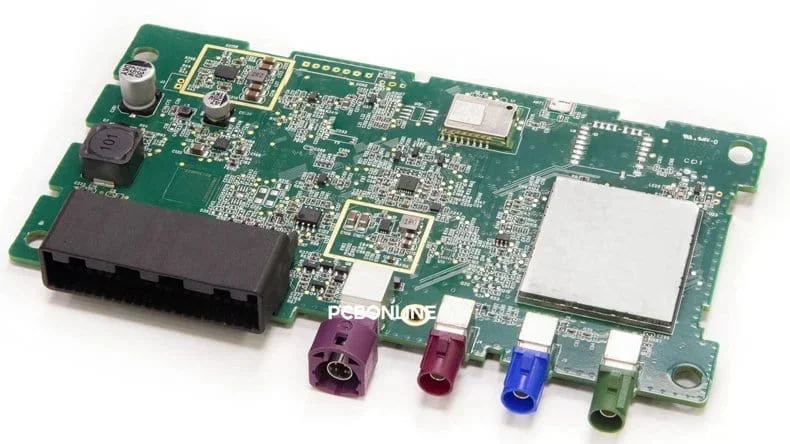
6-layer HDI PCBA for automotive navigation fabricated by PCBONLINE
For various applications that demand impedance control and signal integrity, a 6-layer PCB is preferred. This blog outlines some parameters and processes to consider when designing a 6-layer PCB.
Learn about 6-layer PCB
A 6-layer PCB design requires the end product to satisfy all industry standards and achieve maximum performance. You will need to choose an appropriate substrate material for the multilayer PCB, such as FR4 or Rogers, and check that the material's loss tangent (tan δ) and dielectric constant (εr) meet the application requirements. For complex designs, you can choose PCB design tools like Altium Designer, KiCAD, or Eagle.
The layer stack-up configuration determines the arrangements of the signal, power, and ground layers. A typical 6-layer PCB stack-up is shown below.
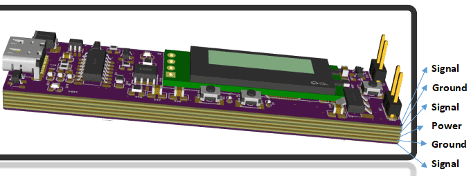
- Top layer: Signal
- Layer 2: Ground plane (GND)
- Layer 3: Inner signal layer (high-speed or sensitive signals)
- Layer 4: Power plane (VCC)
- Layer 5: Ground plane (GND)
- Bottom layer: Signal
When designing a 6-layer PCB, ground/power planes, signal integrity, and impedance control are of top priority.
- Ground and power planes: Place ground and power planes next to each other to reduce the loop inductance.
- Signal integrity: Do not route high-speed signals on layers next to each other to minimize crosstalk.
- Controlled impedance: Ensure dielectric thickness and material properties do not vary significantly.
6-layer PCBs can suffice a wide range of applications, including embedded systems, communication devices, IoT devices, RF systems, high-speed digital circuits, etc.
6-layer PCBs provide many benefits for a mid to high-end application project. Their benefits are as below.
- Signal integrity: Enhanced layer combination leads to reduced noise and crosstalk.
- Thermal management: Better heat dissipation.
- Compact design: Reduces size without compromising the complexity of the circuitry.
- Compliance with EMI/EMC: Enhanced shielding and isolation provide better EMI.
6-Layer PCB Design
The requirements of 6-layer PCB design are:
- Delineate the performance and functionality requirements of the circuit.
- Pinpoint high-speed and sensitive components.
- Identify the voltage ranges and power application requirements.
The general 6-layer PCB design process is below.
Step 1. Schematic design
First, one must diagram the circuit.
Components should be attributed to their appropriate footprints.
Specify net and electrical connection assignments.
Step 2. Components placement
Organize components by their purpose and their roles in the signal flow.
Group like parts together (decoupling capacitors are placed around the ICs, etc).
Consider mechanical and thermal constraints in the design.
Step 3. Allocation of layers
Designate layers of the PCB to power, ground, and routing of signals.
Reserve at least one layer for a ground plane, which can be used as a reference signal.
Ensure that the ground return path for high-speed signals is uninterrupted.
Step 4. Routing
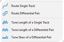
Begin with routing the most significant signals first, for instance, the differential pairs and high-speed signals.
Maintain the trace width and spacing equal for regulated impedance.
To minimize signal loss, minimize the use of vias.
Step 5. Power distribution network (PDN)
For power and ground, use polygons or wide traces.
Place decoupling capacitors moderately on power pins.
A consistent copper distribution can eliminate noise from the power planes.
Step 6. Signal integrity analysis
Employ simulation tools to analyze signal channels for possible crosstalk, reflections, and impedance mismatches.
Considerations in 6-Layer PCB Design
When designing the 6-layer PCB, consider high-speed signal integrity, thermal management, EMC, and the vias.
High-speed signal design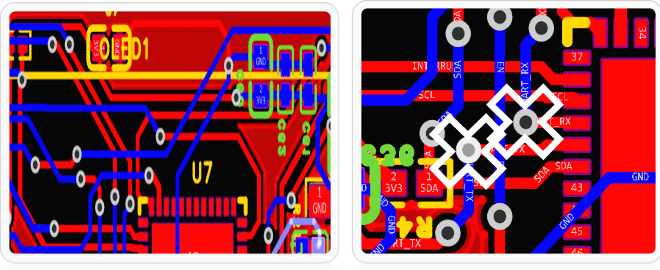
Employ microstrip or stripline designs for defined impedance.
Employ 45-degree angles when tracing bent lines. Avoid sharp corners.
For differential signals like clock or data, ensure the traces are of equal lengths.
Managing thermal effectsIncorporating thermal vias under active components is recommended for better heat dissipation.
In areas of the board that are not being used, copper pours may be placed to aid in the transfer of heat.
Reducing EMC/EMI effectsWhen routing signal traces, reduce their length and keep them in a straight line.
Place the decoupling capacitors as close to the Integrated Circuits as possible.
Do not use segmented ground planes, to avoid ground loops.
Via strategyFor high-speed communication, resist the use of vias to minimize parasitic capacitance and inductance.
Use tented vias' to prevent leakage of solder in the vias amid assembly.
6-Layer PCB Design Validation and Prototyping
Before starting PCB prototyping, the designer needs to confirm that the additional manufacturing files created alongside the PCB comply with the final checks, also known as the design rule check. It normally includes:
Design rule check (DRC): Running DRC helps in identifying spacing, trace width, and the clearance that will be applied in the PCB design tool needed.
Electric rule check (ERC): Verifying the pins assignments and connections with the nets.
After the final check verification, you can submit all the required Gerber files, drill files, stack up, and other relevant documents and information to the PCB manufacturer PCBONLINE. PCBONLINE will do the design for manufacturing (DFM), PCB prototyping, and test the performance and functionality of the prototype. By employing network analyzers and oscilloscopes, the PCB manufacturer measures the signals of the PCBs.
After the prototyping and testing, you can go forward to the PCB fabrication and assembly stage. The one-stop PCBA manufacturer PCBONLINE will complete the bulky PCB manufacturing and assembly for your 6-layer PCB project. After PCB assembly, PCBONLINE will conduct the functional testing to ensure the functionality of the board meets the demanded specs, environmental testing to begin with will prioritize cycling, thermal, humidity vibration, and compliance testing to ensure industry specifications are met like IPC, UL and other standards.
One-stop 6-Layer PCB Manufacturer PCBONLINE
If you need R&D, prototyping, 6-layer PCB manufacturing, PCB assembly, and comprehensive testing and value-added services, you can work with the one-stop advanced PCB manufacturer PCBONLINE.

Founded in 1999, PCBONLINE has two large advanced PCB manufacturing bases, one PCB assembly factory, stable supply chains, and an R&D team.
PCBONLINE provides turnkey electronics manufacturing services for 6-layer PCB projects, including software and hardware R&D, PCB prototyping, PCB manufacturing, component sourcing, PCB assembly, PCBA functional testing, thermal aging, IC programming, enclosures, and box-build assembly.
PCBONLINE offers free one-on-one engineering support and DFM for 6-layer PCB projects, ensuring the smooth manufacturing process and successful results of the boards and end devices.
Various 6-layer PCBs custom meet your project demands, such as FR4 PCBs, flexible PCBs, rigid-flex PCBs, Rogers high-frequency PCBs, HDI PCBs, and copper-based PCBs.
High-quality 6-layer PCB manufacturing certified with ISO 9001:2015, ISO 14001:2015, IATF 16949:2016, RoHS, REACH, UL, IPC-A-600 Class 2/3, and IPC-A-600 Class 2/3.
When your 6-layer PCB project goes to the bulky production stage, PCBONLINE refunds the fees of R&D, prototyping/sampling, and PCBA functional testing.
Besides 6-layer PCBs, you can order PCBs from 1 to 64 layers from PCBONLINE. To get a quote, please contact info@pcbonline.com.
Conclusion
Creating a 6-layer PCB entails thoughtful strategy, thorough proofing, and coordination with your PCB manufacturer. This blog provides general considerations in a 6-layer PCB. An adequate 6-layer PCB design will decrease risks, reduce expenses, and guarantee that the product development cycle is successful. To have your 6-layer PCB project manufactured under one roof, contact the one-stop PCBA manufacturer PCBONLINE.
PCB fabrication at PCBONLINE.pdf


