
As technology evolves, the demand for reliable 8-layer PCBs (printed circuit boards) has surged. These multilayer PCBs offer robust signal integrity, thermal dissipation, and electromagnetic interference (EMI) in telecommunications, aerospace, and computing industries.
This blog delves into the process of designing 8-layer PCBs, offering step-by-step insights with an example project the Gigabit Networking Router 8-layer PCB.
In this article:
Part 1. How to Design 87-Layer PCBs: Designing a Gigabit Networking Router PCB Part 2. Why Choose an 8-Layer PCB? Part 3: One-stop 8-Layer PCB Manufacturer and Assembler PCBONLINEHow to Design 8-Layer PCBs: Designing a Gigabit Networking Router PCB
Designing an 8-layer PCB is a complex but highly rewarding process that requires careful planning, precision, and expertise at every stage. It involves a detailed approach, starting with the stackup design, which defines the arrangement of the layers and their materials for optimal signal integrity and performance.
In this blog, we will focus on designing a Gigabit Networking Router PCB as a real-world application. This project exemplifies the challenges and techniques of creating a high-performance 8-layer PCB.
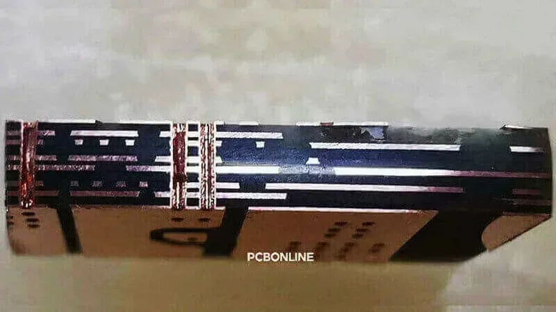
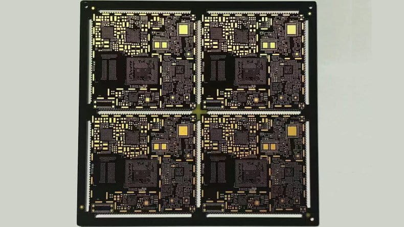
Final design of the 8-layer Gigabit Networking Router PCB
1. Define Design Objectives
Start with a clear understanding of project requirements. For the Gigabit Networking Router PCB, the key objectives are:
- Support gigabit-speed Ethernet signals.
- Fit within standard router casings.
- Efficiently dissipate heat from multiple processors.
Defining these goals early ensures the design meets performance, size, and thermal specifications.
2. Develop the Stackup
A well-designed stackup is crucial for the PCB's performance. For the router project, the 8-layer PCB stackup included:
- Top Layer: High-speed signal traces (Ethernet lanes)
- Layer 2: Ground plane for signal shielding.
- Layer 3: Low-priority signal routing.
- Layer 4: Power distribution.
- Layer 5: Power plane for critical ICs.
- Layer 6: High-speed signal routing.
- Layer 7: Ground plane for shielding.
- Bottom Layer: Mixed-signal routing for auxiliary components.
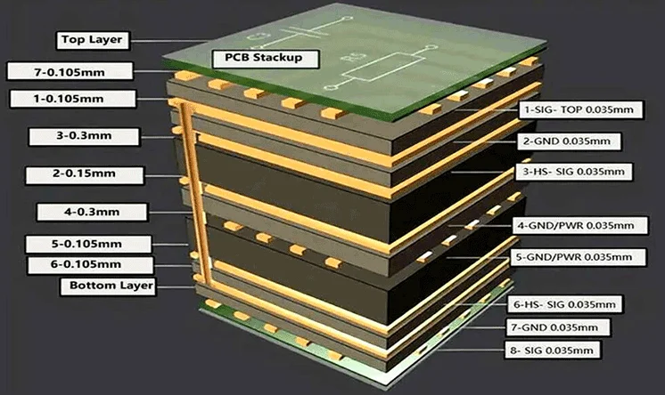
8-layer PCB stackup for Gigabit Networking Router
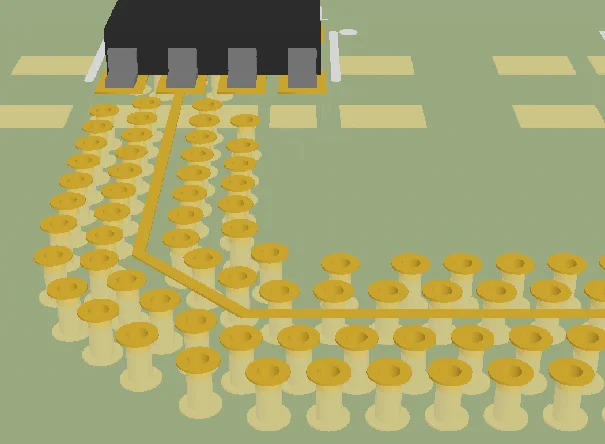
3. Optimize Signal Integrity
- Controlled impedance: Ensure trace width and spacing align with impedance requirements.
- Differential pair routing: Route Ethernet signal pairs together with consistent spacing.
- Short signal paths: Minimize propagation delays and signal loss.
Signal integrity is especially critical in high-speed designs where even minor noise can cause significant data errors.
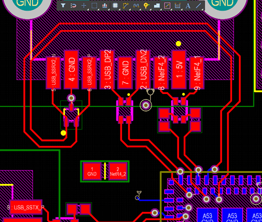
Optimizing signal paths for Gigabit Router-speed performance
To refine performance further, consider:
- Blind and buried Vias: Save space while maintaining layer connectivity.
- Microstrip and stripline routing: Ensure controlled impedance.
- Layer symmetry: Prevents warping during fabrication.
Advanced techniques can significantly enhance performance, especially for boards operating in demanding conditions.
4. Address Thermal Management
Thermal management and EMI (electromagnetic interference) considerations are essential to ensure the PCB operates efficiently without overheating or experiencing signal disruptions. These factors become increasingly important as the complexity of the design grows, especially in high-speed applications like a Gigabit Networking Router PCB.
Efficient heat dissipation prevents overheating and extends the board's lifespan. Techniques include:
- Thicker copper layers: Use 2 oz copper for ground and power planes.
- Thermal vias: Place beneath processors to transfer heat to inner layers or heatsinks.
- Symmetric stackup: Reduces thermal warping during operation.
Thermal considerations also influence material selection, ensuring the board can endure varying operational temperatures.
5. Reduce Electromagnetic Interference (EMI)
EMI can disrupt high-speed circuits. Strategies to mitigate it include:
- Stitching vias: Enhance ground plane shielding.
- Decoupling capacitors: Stabilize power delivery by reducing noise.
- Layer separation: Separate analog and digital signals to limit interference.
Proper EMI management ensures the board complies with regulatory standards and reduces the risk of malfunction.
6. Validate PCB Thickness
PCB thickness influences mechanical stability and signal performance. For the router project:
- A standard 1.6mm thickness was selected for stability.
- Dielectric layers were optimized for impedance control.
Careful selection of board thickness and dielectric properties also impacts cost-effectiveness during PCB fabrication.
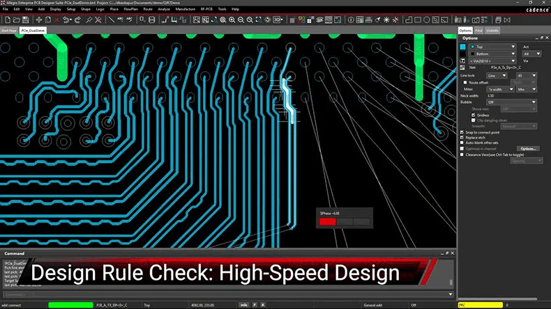
7. Design Validation
Before sending your 8-layer PCB design for manufacturing, rigorous testing is essential:
- Thermal simulations: Identify hotspots and optimize heat distribution.
- Signal integrity tests: Verify the stability of high-speed traces.
- Design Rule Checks (DRC): Ensure the design complies with manufacturing constraints.
Validation ensures that all aspects of the design meet functional and regulatory requirements, avoiding costly reworks.
Why Choose an 8-Layer PCB?
The 8-layer PCB is a favorite among engineers because it offers:
- Enhanced signal integrity: Supports high-speed data transmission with reduced noise.
- EMI reduction: Provides shielding layers to limit interference.
- Compact layouts: Enables dense component placement without compromising functionality.
- Improved thermal management: Incorporates heat-dissipating layers to handle high-power components.
Additionally, 8-layer circuit boards allow designers to balance electrical and mechanical constraints, ensuring reliability even in challenging environments.
Applications of 8-Layer PCBs
Beyond routers, 8-layer PCBs are used in:
- Telecommunication Equipment: For high-speed data transmission.
- Medical Devices: Supporting advanced imaging and diagnostic tools.
- Aerospace Systems: Managing complex signal routing and power distribution.
- Automotive Electronics: Handling infotainment systems and driver assistance technologies.
- The versatility of these boards makes them a staple in cutting-edge innovation.
One-stop 8-Layer PCB Manufacturer and Assembler PCBONLINE
If you need R&D and electronics manufacturing or once you complete your 8-layer PCB design, you can work with the one-stop advanced PCB and PCBA manufacturer PCBONLINE.

Founded in 1999, PCBONLINE has two large advanced PCB manufacturing bases, one PCB assembly factory, stable supply chains, and an R&D team.
PCBONLINE has strong 8-layer PCB manufacturing capabilities, including R&D, prototyping, PCB fabrication, component sourcing, PCB assembly, PCBA value-added, and box-build assembly.
You can order any types of 8-layer PCBs from PCBONLINE, including FR4 PCBs, HDI PCBs, copper-based PCBs, flexible PCBs, rigid-flex PCBs, and high-frequency PCBs.
PCBONLINE offers free design for manufacturing (DFM) and one-on-one engineering support to ensure the success of your 8-layer PCB design and manufacturing.
PCBONLINE can do the R&D for your project or take part in your project's development from the early stage to reduce the fabrication costs from the perspective of an optimum 8-layer PCB design.
High-quality 8-layer PCB manufacturing certified with ISO 9001:2015, ISO 14001:2015, IATF 16949:2016, RoHS, REACH, UL, and IPC-A-600 Class 2/3.
Besides 8-layer PCBs, PCBONLINE provides PCB fabrication from 1 to 64 layers. To get a quote for your multilayer PCB and PCBA project, please contact info@pcbonline.com.
Conclusion
Through thoughtful integration of components and careful layer routing, the 8-layer PCB design maximizes performance while maintaining reliability and durability under varying environmental conditions. For professional assistance with your 8-layer PCB design, it's crucial to work with experienced experts like PCBONLINE to provide specialized PCB solutions.
PCB fabrication at PCBONLINE.pdf


