Most PCBs are 1-layer PCBs, 2-layer PCB, or multilayer PCBs with even-number layers, such as 4-layer, 6-layer, 8-layer...even 100-layer PCB.
However, have you ever used or designed a 3-layer PCB?
3-layer PCB does exist and has already been used in many industries.
There are not only 3-layer PCBs but also other multilayer PCBs with odd-number layers, such as 5-layer and 7-layer PCBs.
But 3-layer PCBs and other odd--number-layer PCBs are rarely used.
Why is a 3-layer PCB rarely used? This article answers this question and gives a comprehensive introduction to 3-layer PCB.
Part 1. Why is 3-layer PCB Rarely Used?
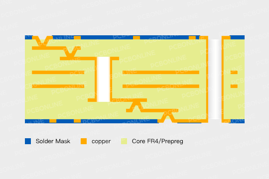
A 3-layer PCB is a multilayer PCB having 3 copper circuit layers, and the base materials can be FR4, PI (polyimide), PET (polyester), ceramic, etc.
A 3-layer PCB is rarely used because it is easy to warp during fabrication.
In many cases, if a four-layer circuit board can meet the needs, we will design a four-layer PCB instead of a three-layer PCB.
If unnecessary, we do not use 3-layer PCB. The reasons are:
1. Asymmetric structure may cause warpage
A 3-layer PCB has an asymmetric PCB structure.
Most 3-layer PCBs are FR4-based. Their PCB fabrication method is the same as 4-layer PCB manufacturing, but only that an inner copper foil layer is etched out totally.
Along the PCB core's middle line, the two sides have different copper layers, and their thicknesses are different.
In the lamination process, the different thicknesses on two sides of the core can cause the circuit board to warp or even pop.
2. The price of 3-layer PCB is the same as 4-layer PCB
Usually, the PCB manufacturers charge the same fee for 3-layer and 4-layer PCBs.
Why does 3-layer PCB fabrication have the same price as 4-layer PCB?
A FR4 3-layer PCB is made out of a 4-layer PCB whose inner layer is extra etched away.
Although it has less copper than a 4-layer PCB, the materials needed for PCB fabrication are the same amount as a 4-layer PCB.
Nevertheless, 3-layer PCB fabrication requires one more step - removing an inner copper layer.
Because of the potential warpage, the same PCB fabrication method (for FR4 3-layer PCB), and the same price as the 4-layer PCB, 3-layer PCB is rarely used.
Part 2. Odd-Number-Layer PCB Design
In PCB design, a symmetrical structure along the middle line is essential. This requires the prepreg, copper layer, copper thickness, and circuit graphic distribution on the two sides as balanced as possible.
With a symmetrical PCB structure, you can reduce the FR4 PCB fabrication cost and avoid warpage.
If your PCB design is an odd-number-layer PCB, you can try the below tips to achieve a symmetrical PCB structure.
Add a signal layer: If the PCB's ground layer is in an even-numb layer and the signal layer is in an odd-number layer, you can add an extra signal layer to the PCB.
Add a blank signal layer near the PCB stickup's middle line: You can a blank signal layer near the middle line to make the two sides have the same copper layer. In this way, the PCB has a symmetrical structure.
If you want to design a 3-layer flexible PCB or 3-layer ceramic PCB, you still need to make the thicknesses of the two sides of the middle line as close as possible.
Part 3. 3-Layer PCB Fabrication
A 3-layer FR4 PCB has the same fabrication process as a 4-layer PCB, but it requires to removal of an inner copper layer by etching.
Typically, the fabrication process for 3-layer FR4 PCB is:
Cut laminate: Prepare the PCB laminates for PCB fabrication.
Etch an inner layer away: Remove an inner copper layer by etching.
Inner layer circuit generation: Coat the inner copper layer with a photoresist, transfer the circuit image to the copper foil by imaging, etch the unwanted copper areas to generate the circuits, and have an AOI (automatic optical inspection) to check the circuits.
Lamination: Attach the prepreg and outer copper layers on the PCB core layer, and laminate them to be a 3-layer PCB.
Drill and electroplate PTH holes: mechanically drill the FR4 PCB and electroplate the through hole walls with copper by VCP (vertical continuous plating).
Outer layer circuit generation: coat the outer copper layer with photoresist, transfer the circuit image to the copper foil by imaging, electroplate copper on the circuit traces to increase the copper thickness, electroplate tin on the circuit traces to protect them, etch the non-circuit copper area away, remove the tin film on the copper circuit traces, and have an AOI (automatic optical inspection) to check the circuits.
Surface finish, solder mask, and silkscreen: Apply surface finishes on the copper PCB pads, spray solder masks on the PCB, and print silkscreens (the characters and symbols) on the 3-layer PCB.
Profile and test: Profile the PCB panel to form the PCB shapes, and have the flying probe test, electrical test, and sample test.
The above is the fabrication process of a 3-layer FR4 PCB.
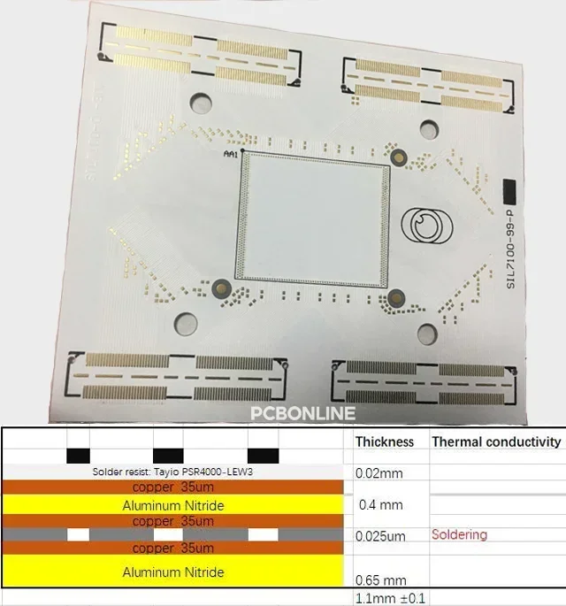
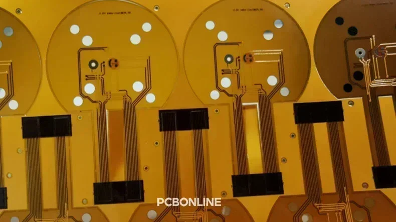
At the advanced PCB manufacturer PCBONLINE, 3-layer ceramic PCB and 3-layer flexible PCB are also available.
The manufacturer must have professional expertise and rich experience to control the lamination process.
Otherwise, the 3-layer PCB can warp or even break due to the unsymmetrical prepreg on the two sides.
Part 4: 3-Layer PCB Manufacturer and Showcases
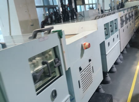
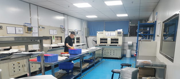
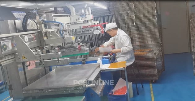
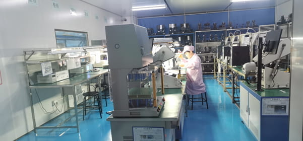
PCBONLINE is a professional PCB manufacturer providing 3-layer PCB fabrication and assembly of any type.
PCBONLINE is a one-stop PCB manufacturer that is ISO-verified. It has two advanced PCB manufacturing bases and one PCB assembly factory.
PCBONLINE provides 3-layer PCBs of any kind, such as 3-layer FR4 PCB, ceramic PCB, and flexible PCB.
It provides one-stop 3-layer PCB fabrication and assembly from prototype to bulk production.
At PCBONLINE, the engineer with more than 20 years of experience offers one-on-one engineering support throughout your project.
PCBONLINE can optimize your 3-layer PCB design and ensure the success of PCB fabrication and assembly.
Low-cost and high-quality 3-layer PCB because PCBONLINE is a source factory manufacturer.
Here, you can check some showcases of 3-layer PCB manufactured by PCBONLINE.
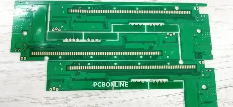
PCBONLINE has served many 3-layer PCB projects for military, aerospace, medical, automotive, communication, industrial, and consumer electronics. If you need 3-layer PCBs, contact PCBONLINE at info@pcbonline.com.
Conclusion
This blog gives a comprehensive introduction to a 3-layer PCB, including its design and fabrication. A 3-layer PCB is rarely used because it has an unsymmetrical structure and is easy to warp. To have a 3-layer PCB manufactured and assembled that can yield successful results, work with a reliable and low-cost PCB manufacturer PCBONLINE.