
Question: How can we find a good PCB manufacturer in China? What is the PCB manufacturing process of a multilayer PCB?
No worries! This PCB manufacturing guide explains the PCB fabrication process, PCB testing, and failure analysis, and also some related content about PCB manufacturing.
PCB is a laminated board with alternating layers of dielectric and conductive traces. It is designed for the electrical and mechanical connection of various electronic components.
PCB comprises mounting holes and the contact pad for mounting pin or planar components. The outer sides of the circuit board are usually covered with solder masks and markings.
How is a PCB manufactured? Check the PCB manufacturing process below.
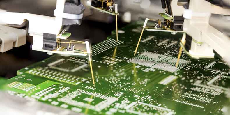
1. What is the PCB Manufacturing Process?
![]()
PCB fabrication is the process of etching copper to generate copper circuit traces on the non-conductive laminate material sheets, laminating the layers, and interconnecting different circuit layers with copper plating holes.
The whole process of manufacturing PCB can be divided into four phases:
- Manufacturing a blank (foil material)
- Processing workpieces to obtain the necessary electrical and mechanical types.
- Assembly components
- Testing
Normally, the manufacturing of PCB is understood only as the processing of a workpiece.
The PCB Manufacturing Steps are:
Step 1. Cut laminate: The laminate is a substrate material that consists of fiberglass or composite. The first step in PCB manufacturing is to split the laminate into pieces in the panelized board's size.
Step 2. Film making: For each circuit layer, a film is generated to create the circuit pattern on the PCB.
Step 3. Inner layer generation: The inner layer of the PCB is produced by laminating copper foil to the laminate. Using the film in Step 2 under ultraviolet light, the circuit pattern is imaged onto the copper layer. In the etching process, the unwanted copper is removed, leaving behind the desired circuit pattern.
Step 4. Drilling: Next, the PCB is drilled to create holes that connect different layers of the PCB.
Step 5. Electroless copper deposition: After drilling, the PCB is plated with a thin layer of electroless copper to provide a conductive layer for the subsequent electroplating steps.
Step 6. Lamination and bonding: The outer layers of the PCB are produced by laminating copper foil to a substrate material, followed by an imaging and etching process. The layers are then bonded together with a lamination process.
Step 7. Electroplating: A copper layer is then electroplated onto the outer layers of the PCB to provide additional conductivity and to build up the thickness of the conductive layers.
Step 8. Soldermask application: A soldermask is applied to the PCB to protect the conductive layers. A surface finish is applied on the contact pads for soldering components.
Step 9. Silk screen printing: Finally, the PCB is silk-screen printed with component designators, logos, and other identifying marks.
Step 10. Testing: The completed PCB is then tested to ensure that it meets the required functionality and performance standards.
Flexible PCB manufacturing, aluminum PCB manufacturing, and ceramic PCB manufacturing are different from the above steps. If you want to get an insight into these PCBs' manufacturing process, click the corresponding link to read the article.
2. PCB Testing and Failure Analysis
Enterprises with metallographic examination, electrical testing, endoscopic examination, and thermo-mechanical analysis have made great progress in understanding quality control problems.
It is recognized that it is necessary to make a detailed analysis of all elements of electronic equipment. At the one-stop PCB manufacturer, there are full equipment and processes for PCB/PCBA testing and inspection.
- Tensile testing machines for determining the ductility of galvanically deposited copper in the holes of PCBs;
- Machines for determining the shear strength of rations;
- Hydrostat for expert determination of the cleanliness of the boards from technological contamination;
- Electrical measuring instruments for testing electrical insulation and conductivity;
- Means of functional, parametric, and diagnostic control of electronic means for PCBs, printed circuit assemblies and blocks, and box-builds.
Working with PCBONLINE, all of the boards will go through functional tests and aging tests which ensures high quality. PCBONLINE makes sure no inferior PCB or PCBA flows into our customer end. Below is the video of the PCBA test.
3. Why is PCB Prototyping Necessary for PCB Manufacturing?
The main goal of PCB prototyping is to test how consistent the user journey is and to identify and solve obstacles that may arise in the PCB manufacturing process.
![]()
The fabrication process of PCB prototypes is the same as massive manufacturing. So are PCB testing, PCB assembly, electronic components, and value-added services on the samples. This is to ensure the quality of massive PCB manufacturing.
Though the unit price of PCB prototypes is higher than massive manufacturing, it ensures the smooth project fabrication process of massive PCB manufacturing.
4. One-Stop Advanced PCB Manufacturer From Prototypes to Massive Manufacturing
PCBONLINE has been a one-stop advanced PCB manufacturer since 1999. They have two large PCB manufacturing bases and one PCB assembly factory. And they support all stages of your PCB project from prototypes to mass production until you get end products.
It manufactures and assembles any complex PCBs at any volume that you need them.
All PCBs, PCBAs, and box-builds manufactured by PCBONLINE are strictly quality-controlled to be compliant with ISO, IATF, RoHS, UL, REACH, and IPC standards.
It is a source-factory PCB manufacturer and provides competitive prices.
It provides free PCB DFM and DFT, PCBA DFA, and box-build DFX.
The quickest build time with the fastest delivery in only 8 working hours.
PCBONLINE can optimize your design to reduce the fabrication price without quality sacrifice.
PCBONLINE is not only a PCB manufacturer. It has rich R&D experiences and can take part in your project development in the early design stage. If you want to start your project journey, feel free to contact PCBONLINE by email at info@pcbonline.com.
PCBONLINE's capability:
- Layer: 1 ~ 64
- Laminate: FR4 of any Tg, polyimide, polyester, aluminum, copper, ceramic (AlN and Al₂O₃), and PTFE (Teflon)
- Surface finish: OSP/HASL/LF HASL/ENIG/immersion tin/immersion silver/hard gold plating/carbon ink/silver plating
- Board thickness: 0.15mm ~ 3.2mm
- Max board size: 500mm × 580mm
- Copper thickness: (inner finish copper) 1/3oz-4oz, (outer finish copper) 1/3oz-14oz
- Min. line width/spacing: 0.0635mm/0.0635mm
- Min. CNC drilling size: 0.15mm
- Min. laser drilling size: 0.075mm
- HDI stack up: 1+N+1, 2+N+2, 3+N+3
Conclusion
The PCB manufacturing process is a specialized process for creating high-performance and complex PCBs with a high level of miniaturization and functionality. If you need PCBs, work with a reliable source-factory manufacturer PCBONLINE that provides one-stop PCB services.


