
When you come across any mass-produced electronic device, it is almost certain that there is a PCB inside of it that has gone through rigorous testing procedures. These PCB assembly testing procedures are designed to identify and prevent PCB manufacturing faults, faulty components, soldering issues, functionality issues, component alignment, and quality issues to ensure the end product has the expected lifetime.
Let's see all kinds of PCB assembly test methods now!
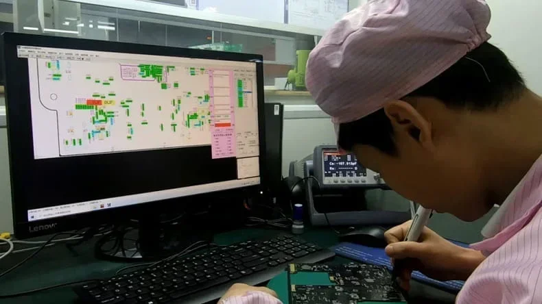
Part 1: Methods of PCBA Testing
There are various methods for PCB testing depending on their complexity. Here we discuss the most common and widely used methods for testing PCBAs in the assembly process.
- In-Circuit Testing Methods
- Automated Optical Testing
- Boundary Scan Method
- Built-in-Self Test
- Burn-In Testing/Aging Testing
- X-ray Inspection
- Functional Testing
- Other Functional Tests
In-Circuit Testing (ICT)
Stage: at the end of the PCB assembly
Purpose: capture manufacturing defects and validate PCB functions according to the specifications
In-circuit testing (ICT) is a combination of different testing instruments into one. The test system connects to the PCB via test probes which connect to test points in the PCB. This electrically tests circuits and components against critical values.
The most common defects that can be identified with ICT are solder shorts, missing components, component failures, lifted pins, component shifts, and poor soldering issues.
Here are the common electrical measurements by ICT probes: open circuit tests, short circuit tests, resistance measurements, capacitance measurements, inductance measurements, diode/direction of current measurements, and voltage level measurements.
There are two test options to choose from for in-circuit testing - the standard bed of nails test and the flying probe test.
Standard Bed of Nails In-Circuit Test
Suitable for: PCBs except for modern densely packed boards
Advantages: testing coverage of about 85-98%; can run many parallel test measurements at once
Disadvantages: the high cost of the machine; difficulty in updating beds of nails
In-circuit testing machines have fixtures used to interface the assembled PCB with the tester. A fixture consists of probes (needles) that are configured to connect specific test points in the PCB. The probes are connected to fixture interface pins by fixture wires. These wires provide flexibility to change the probes for different PCB test points. Fixture interface pins connect with tester module interface pins. The tester drives a sequence of different signals to the PCB and receives signals back through this interface. The tester checks the received signals from the PCB and compares them with standard signals for the given PCB to detect any anomalies. In-circuit testing machines have. Due to that, the machine can't access test points of modern densely packed PCBs, and PCBs are more and more advanced, so this method is used less and less frequently.
Flying Probe In-Circuit Test (FICT)
![]()
Suitable for: prototype PCBs, low to mid-production PCBs
Advantages: no need for test fixtures of each PCB variant
Disadvantages: much longer test cycle time
Flying probe testing is also an in-circuit test system that uses two or more probes that can move around the PCB board and lower probes on test pads to conduct its tests. It conducts tests in a series of manners. This method is also applicable to high-density PCBs, PCBs that cannot fit into standard ICT test fixtures, and PCBs with small size contacts down to 0.2mm test pitch.
Automated Optical Inspection (AOI)
![]()
Stage: after reflow soldering in SMT assembly
Suitable for: All PCB in any volume
Advantages: extremely fast and precise
Disadvantages: test only the surface of the assembly
This method uses multiple cameras or microscopes to get images of the PCB assembly. The images are then compared with reference images with the help of software. This method is also able to verify the quality of the end product and provide a visual track of the PCB assembly process. The automated Optical Testing method replaces visual inspection by humans with more precision and speed.
Common flows that can be detected with AOI are missing components, misplacement, misalignment, overall quality, and PCB assembly dimensions.
Boundary Scan Method
Stage: after the whole PCB assembly
Suitable for: integrated circuit chips
Advantages: can test JTAG-compatible components together
The boundary-scan method, also known as JTAG (IEEE Std 1149.1), is a debugging method for integrated circuit (IC) chips. PCBs that support boundary scans have a JTAG interface port that allows access to ICs and embedded logic. JTAG test uses a shift register that is built into each boundary-scan compatible device. In these devices, there is a boundary-scan cell adjacent to each I/O pin of the IC. When in shift register mode, data is transferred along with these cells. Each JTAG-compatible IC has pre-defined exit and entry points for this test data to enter and exit. Because of this, many JTAG-compatible components can be chained together to test. Under normal operating conditions, these boundary scan cells have no effect. When in test mode, the JTAG boundary scan can even monitor the returning data from the shift register chain and determine whether the PCB assembly has passed the JTAG test.
The JTAG interface is formed with several control and data lines. Following is the common technical jargon about JTAG:
- TAP (Test Access Port) - These are pins associated with the test access controller.
- TCK (Test Clock) - This is the clock signal pin for the timing of the boundary scan system.
- TDI (Test Data Input) - Test vector (data stream) injected into the PCB through this pin.
- TDO (Test Data Output) - This pin receives data (test vector) from the boundary scan registers.
- TMS (Test Mode Select) - This input determines the state of the TAP controller.
- TRST (Test Reset) - This is an optional reset pin. It resets the TAP controller.
Built-in-Self Test (BIST) or Built-in Test (BIT)
Stage: last stage of some PCB assemblies
Suitable for: Batched production PCB
Advantage: highly reliable and, helpful especially when repairing PCB
Disadvantage: complex setup
This is a mechanism that allows the PCB assembly to test itself. Built-in-self test systems not only provide highly reliable tests at production time but also help at later stages like when there is a repair in the PCB these systems can point out where the problem is.
BIST systems reduce the complexity of PCB assembly testing by reducing the test cycle duration and having a complex setup of In-circuit testing (testing with probes) techniques.
Here are examples of BIST systems:
- On-board diagnostics (OBD) in the Automotive field carry self-tests on critical systems to enhance safety and reliability.
- Power-on Self-Test (POST) in computers to ensure every part of the system works as it should.
- Self-test systems in mobile phones test all the sensor's data, camera, and hardware functionalities.
Burn-in testing or Aging Test
![]()
Stage: after the PCB assembly
Advantage: it stimulates the real use of PCBA for long hours
Disadvantages: it costs quite a long time depending on the requirements
This method of testing is to ensure the reliability and survivability of the PCBs under maximum specified stresses and loads. Burn-in testing detects early failures and can be a destructive test for the parts being tested.
Burn-in testing powers up the electronics in the PCB to their maximum rating continuously for 48 to 168 hours depending on manufacturer specifications. If a board fails at this time it is called \"infant mortality\". This test is common for PCBs designed for military and medical applications.
X-ray Inspection (AXI)
Stage: before reflow soldering in SMT assembly
Suitable for: BGA PCB
Advantage: precisely detect internal defects
Disadvantage: high test machine cost
This is an inspection test for detecting defects that are hidden from Automated Optical Inspection methods. For example, AXI is used to inspect solder connections under ball grid array (BGA) packages that have solder joints underneath the chip package. X-ray Inspection is more commonly done on a selected sample basis in the manufacturing process.
This method is also used to inspect silicon wafers for internal defects. AXI is available both as 2D and 3D tests. Generally, this method is considered a very expensive PCB assembly testing method.
Functional Testing
![]()
Stage: after PCB assembly, before aging/burn-in test
Suitable for: batched PCB
Advantage: cover all behaviors of end products or PCB
This is the last testing of a PCB assembly. Here the functional testing machine simulates the PCB's actual behavior and determines the final pass or fail. The functional testing bench is a combination of Test probes, connection cables, power supplies, and test software. Functional test fixture covers PCB behaviors in-circuit testing (ICT) does not. For example, booting up a mobile PCB or bios boot-up of a PC motherboard followed by a built-in self-test (BIST). After the functional testing, the manufacturer has the confidence to give the product warranty for a period in which the product has proven to survive.
Usually, functionality tests of a PCB assembly in a certain PCB domain do not change with every revision. It only changes slightly in every generation. For example, PC motherboard functionality test machines can test different motherboards consisting of different revisions because the main functionalities remain the same for generations.
Other Functional Testing
In addition to the above functional tests, some unique tests are focused on the products or PCB’s behavior in the end-user environment. These can vary greatly by PCB and end product.
IP rating tests, drop tests, water resistance tests, voltage surge tests, Electromagnetic interference (EMI) tests, and radio-frequency interference (RFI) tests are some common tests conducted.
Other PCB assembly testing
There are some other PCB assembly tests in addition to the main ones. These are useful for tuning the manufacturing process to provide a better quality product.
- Peel test: This test measures the strength required to peel off the lamination from the PCB.
- Solder float test: Evaluates the thermal stress on the PCB.
- Solderability tests: This measures how well metal is wetted by solder and ensures surface sturdiness which can increase the chances of forming a solid reliable solder joint. The most common types of Solderability tests are the "Dip and look" method, the surface mount simulation test, and the wetting balance analysis.
- Micro-sectioning analysis: This analyses the structural characteristics of solder joints and investigates defects and anomalies. It can be applied for both surface mounting technology (SMT) and through-hole technology (THT) PCBs.
- PCB contamination testing: This test investigates Corrosion, Degradation, Metallization, and foreign material contamination in the PCB. Which can cause short circuits and other catastrophic failures.
Part 2: Order PCB Assembly Going through Testings Before Delivery
If you ask a PCB manufacturer to assemble your boards, you must want to get boards that were already been tested before going to your hand. Otherwise, you will have to test them, which is fussy and cozy. Here is a good choice to have your PCBs made, assembled, and tested at once - working with PCBONLINE. This is a one-stop PCB company that is good at advanced circuit boards. You can have them make, assemble, and even design advanced PCBs, and they test your PCB carefully before delivering it to you.
SPI, x-ray testing, AOI, functional testing, and aging testing are conducted default free of charge.
You can require any other PCBA tests from us, like flying probe test, boundary scan, peel test, solder float test, solderability test, micro-sectioning analysis, and PCB contamination testing.
Our experienced engineers can design a build-in-self test system to help you repair easily.
We check your Gerber and BOM carefully before PCB manufacturing and assembly, which reduces possible risk.
We offer free PCB/PCBA samples for batch production.
What PCB Defects Are There to Be Tested?
What are the common faults of PCB assembly that need PCBA testing? The following are some of them for you to read.
Solder BridgesSolder bridging or shorts occur when the solder creates an undesirable conductive path between leads or pins. These solder bridges can be microscopic and could be difficult to detect if there are no proper PCB assembly testing methods in place. If a PCB rolls out an assembly line with a short undetected, it could lead to a burnout PCB trace or blown-up components. The most common cause for Solder bridging is insufficient solder mask between pads and pins. Uneven alignment of components and PCB also can cause solder bridging.
Plating VoidsContamination in the material can cause poorly plated copper inside the through-hole walls on the PCB. This can lead to poor current passes between the PCB layers. It can be avoided by thoroughly cleaning the holes after drilling to wash away any contamination.
Insufficient WettingIdeally, molten solder should cover the leads evenly. Insufficient Wetting is If there is excess solder as mounds (called de-wetting) or areas in the leads that are only partially covered with solder (called non-wetting). Using quality solder and assembly equipment can prevent this issue from happening.
Open Solder JointsThis occurs when there is no solder bond between the component lead and pad. Common causes for this issue are insufficient wetting, the gap between component lead and PCB pad, poor solder paste, and component misalignment.
Component Shift or MisalignmentComponent misalignment can happen in the reflow stage where components float due to insufficient epoxy material to hold them in place. Inconsistent temperatures and mismatches of a component lead to pads that can also cause component shifts.
Bottom Line
This blog illustrates all of the PCBA tests in the electronics world. I am sure you should get familiar with PCBA testing now. If you are considering buying PCB assemblies that have been completely tested, work with PCBONLINE. High-quality PCBA and end products are awaiting you with fast delivery!


