
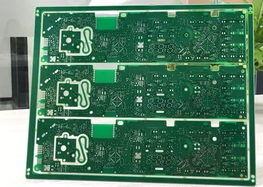
A Printed Circuit Board or PCB is a board with the purpose of connecting electronic components. It consists of alternating layers of conductive copper and layers with non-conductive material for insulation purposes.
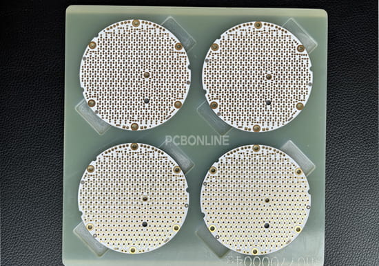
A circuit board can be very simple, with few components mounted, it can also be complex, which takes much effort to design and fabricate, with hundreds of tiny components mounted. Different circuit boards have different features. As you can see below, this is a ceramic PCB that is featured with the ability to withstand high temperatures of more than 1000°C and conduct thermal quickly.
What is PCB?
PCBs are produced from the Gerber files, and Gerber files are generated from schematics diagrams. The PCB makes the connection between the electronic components attached to its surface. There are FR4 PCB and IMS PCB widely used in the electronics market. There are also ceramic circuit boards that are not used so frequently.
When printed circuit boards are made, two methods are used to mount components on the surface of the substrate, called Surface Mount Technology (SMT) and Through-Hole Technology (THT). And the board mounted with desired components is called PCB assembly (PCBA). When PCBA is mounted with the outer covering, it is actually the end electronic product.
The above gives you a general understanding of what a printed circuit board is. There are many types of PCB, for a brief introduction, I will explain its basic structure and general types one by one.
Basic Structure of Printed Circuit Board
The most basic printed circuit boards are the ones that contain copper tracks or interconnects just on one of their surfaces. These sorts of boards are known as 1-layer printed circuit boards or 1-layer PCBs. A single-layer printed circuit board has an inner layer and an outer layer.
In the below illustration, you can see the stack-up of a single-layered printed circuit board.
Now we are ready to briefly review each of the layers of the stack-up:
1. FR4 (Substrate)
PCB substrate can be FR4, metal, or ceramic. FR4 is mainly used and is a reinforced epoxy laminate material. It is the base substrate of the printed circuit boards. It is an extremely durable material and there are different thickness types. Some PCBs, especially the cheaper ones, are made from other materials and they lack FR4 durability.
2. Rigid Copper Clad Laminate (Copper Layer)
The copper layer is a thin foil of copper. It is laminated to the board with adhesive and heat. It is commonly applied on both sides of a double-sided printed circuit board. A two-layered or double-sided board means that there are two copper layers in the structure. You can find PCBs with only one or more than 16 copper layers!
3. Solder Mask
Have you ever wondered why the PCB boards are green? Because of the solder mask layer. This is the top layer above the copper foil, giving the printed boards their green color. The main purpose of this layer is to insulate the copper traces from accidentally contacting any solder or metal. The common color is green, but have in mind that the solder mask could be manufactured in nearly all possible colors.
4. Silkscreen
On top of the solder mask, a white/black silkscreen layer is applied. It is used to insert any numbers, symbols, or letters as instruction like a guideline for people to better understand the board. Again, any color can be used and there are PCBs with yellow, red, or even black silkscreen.
As we now cover all the layers and we have a basic understanding of how the PCB boards are created and how they work, it is time to reveal the different types.
Types of Printed Circuit Boards
The Printed Circuit Boards can be classified and grouped according to multiple numbers of ways. The criteria for the classification of the circuit boards are given below.
- i. Location of the component
The classification of the printed circuit board can be done based on whether the component location is embedded, single-sided, or double-sided.
Single-sided PCBs are the easiest to design. They are used for a variety of applications including radio equipment, calculators, solid-state drive, and simple electronics compared to multi-layered circuit boards.
- ii. The stack-up
According to the stack-up differences, printed circuit boards can be single-layer, double-layer, or multilayered.
When there are four or more layers together, it is called a multi-layered board. They are glued together by specialized glue and carefully secured preventing heat damage. In fact, the largest printed circuit board ever built is over 50 layers thick!
- iii. The design
When the design is considered, the printed circuit boards can be classified as custom, special, and module-based.
- iv. The bending ability
Based on the bending nature and bending capability, the circuit boards are mainly classified as flex, rigid, and rigid-flex.
- vi. The electrical functionality
Based on this criterion of classification, the Printed Circuit Boards can be grouped as microwave, high density, high power, and high frequency.
PCBONLINE, an advanced PCB manufacturer, provides custom PCBs and can meet all your requirements! PCBONLINE has an extremely strong technical strength to manufacture advanced circuit boards, such as HDI, high-frequency, ceramic, multilayered, etc. It provides one-stop PCB manufacturing and assembly, with free PCB and assembly samples.
PCBONLINE's PCB production capability:
- Layer: 1 ~ 42
- Substrate: FR4, aluminum, copper, ceramics, PTFE, polyimide, polyester, and glass
- Surface finishing: OSP/HASL/LF HASL/immersion ENIG/immersion tin/immersion silver
- Board thickness: 0.15 ~ 3.2 mm
- Max board size: 500 × 580 mm
- Copper thickness: (inner finish copper) 1-4oz, (outer finish copper) 1-7oz
- Min. line width/spacing: 0.0635 mm/0.0635 mm
- Min. CNC drilling size: 0.15 mm
- Min. laser drilling size: 0.075 mm
- HDI stack up: 1+N+1, 2+N+2, 3+N+3, 4+N+4
Printed Circuit Board (PCB) Application
Printed circuit boards provide us with a variety of capabilities and they find different applications in almost everything electrical or electronic.
Industrial Use
Many manufacturing facilities have electronic components that require printed circuit boards to achieve the end design. PCBs are found in industrial equipment such as presses, ramps, assembly machines, and more.
In the automotive industry, many vehicle systems such as navigation, media devices, control systems, and monitors are using PCBs.
Printed circuit boards also find applications in medical devices, such as CT scanners, X-Ray screens, and blood pressure monitors. All of the scanning equipment, medical instruments, and monitors contain PCBs.
Home Applications
The most common application of printed circuit boards is in consumer electronics. In fact, PCBs are the heart of every electronic device, such as mobile phones, computers, workstations, navigation, TV, microwave, coffee machine, refrigerator, and even your smartwatch.
What is Next for Printed Circuit Boards?
The PCBs are continuing to drive towards a compact and smaller design with increased capabilities. Some speculations regarding the future of the PCBs may be the integrated circuit chips or the tree-dimensional molded plastic board.
![]()
Most of the predictions for the PCB's future are strongly focused on the following:
-
PCB Auto Places - Most of the printed circuit boards today include an auto-router in their design. The whole idea is to make the automation process easier. Autoroutes are difficult to create and implement, taking a lot of time and work.
The time that the automatization saves is later lost when autoroutes are designed. Many manufacturers are now looking at an auto place as the resolution. Autoplacers make the manufacturing process easier and automatization much faster.
With the idea of integrated CAD systems, PCB design technology is on the rise recently. The auto places need both mechanical and electrical design aspects, the CAD system applies in both realms and it is necessary to make the auto places more beneficial and efficient.
- 3D Printed Electronics - This is probably the most exciting technical invention in the recent decade! It is already beneficial for a variety of industries. I mention this because 3D printing electronics have changed the way we look at electronics forever. That technology will revolutionize the way electronic systems are created in the future, and the same goes for PCBs.
- PCB Cameras - Printed circuit board cameras or also called board cameras are specific in that they are mounted directly on the circuit board. It has to be very small to fit a camera into a PCB. In fact, small enough that it can fit in about any electronic device. That type of camera might be the future for PCB designs.
Conclusion
The content in this article is summarized in an accessible manner so that everyone can get a better sense of PCBs. The truth is that all this is far more complex than it looks and if you are interested to order printed circuit boards, navigate to PCBONLINE, for online quotations and more information.


