
Printed Circuit Boards (PCBs) are the foundation of modern electronic devices. They connect and support components mechanically and electrically. At PCBONLINE, we provide advanced PCB manufacturing for all types of PCBs, from multilayer FR4 PCBs to HDI and ceramic PCBs. While the general production flow follows standardized steps, each PCB type may require unique processes or technologies.
PCBONLINE is an OEM PCB manufacturer for advanced PCB manufacturing. Our article will walk you through how printed circuit boards are made, including the step-by-step general PCB fabrication process and key steps for special PCBs like HDI and ceramic PCBs.
General PCB Fabrication Steps at PCBONLINE
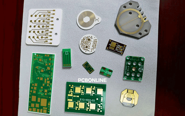
What are considered general PCBs? FR4 PCBs, thick-copper PCBs, aluminum PCBs, and copper-core PCBs are considered general PCBs. Advanced PCBs include HDI PCBs, ceramic PCBs, flexible PCBs, rigid-flex PCBs, and high-frequency PCBs.
The fabrication processes of advanced PCBs do not differ from general PCB fabrication that much. Below is how printed circuit boards are made step by step.
1. Cutting the laminate
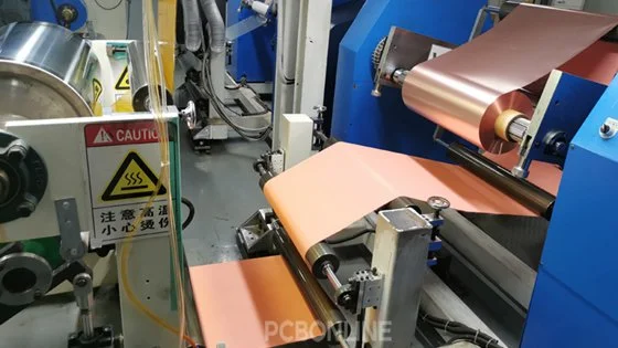
The process begins with copper-clad laminates (CCLs), which are sheets of insulating material (often FR4 epoxy glass) clad with copper foil on one or both sides. Based on design specifications, we cut these laminates into panels that fit the production line. Copper thickness can vary depending on current requirements (e.g., 0.5 oz, 1 oz, 2 oz). The panels are carefully trimmed to avoid burrs or irregular edges, which could affect quality downstream.
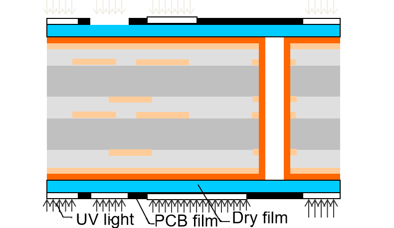
2. Inner layer circuits
For multilayer PCBs, inner circuits are created before lamination:
- Surface pretreatment: The copper surface is chemically cleaned and roughened to improve adhesion.
- Dry film lamination: A photosensitive dry film is heat-laminated onto the copper.
- Exposure: A phototool (film) transfers the circuit pattern onto the dry film using UV light. For inner layers, a negative film is used; for outer layers, a positive film.
- Development: An alkaline solution (Na₂CO₃) removes unexposed photoresist, leaving the circuit protected.
- Etching: Unprotected copper is etched away, forming traces.
- Film removal: The remaining resist is stripped with NaOH.
- AOI (automated optical inspection): High-resolution optical systems inspect for shorts, opens, and defects in fine traces.
This results in finished inner circuit layers, which will later be laminated together.
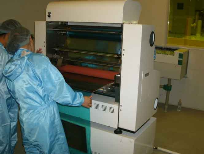
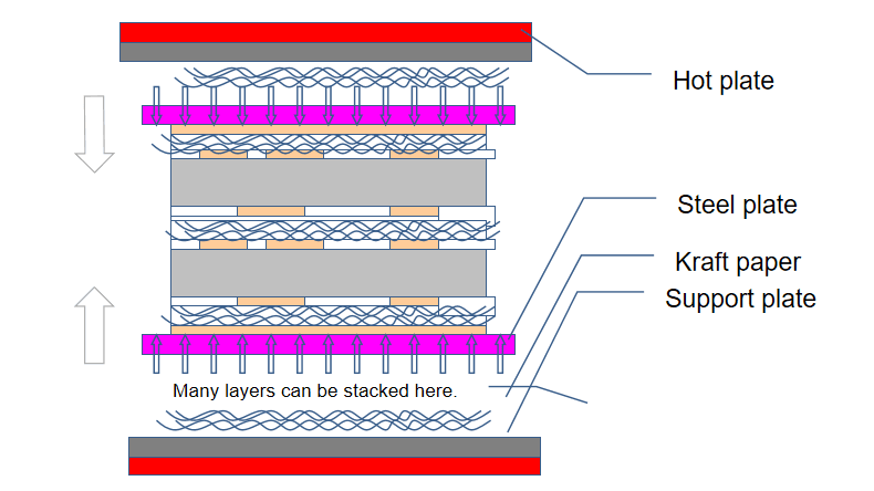
3. Lamination
Lamination bonds the inner layers, prepregs, and copper foils into a solid multilayer PCB:
- Brown oxide treatment: Roughens copper surfaces to enhance resin bonding.
- Pre-stacking and riveting: Multiple inner layers are aligned with prepreg sheets and temporarily fixed to prevent misalignment.
- Layer stacking: Copper foils are placed on the outer sides, forming the outermost layers.
- Lamination press: Under heat and pressure, resin in the prepreg melts and flows, bonding everything together. Materials like kraft paper and steel press plates ensure uniform pressure and flatness.
- Post-lamination processing: Positioning holes and preliminary profiles are made to align with later steps.
4. Drilling
CNC drilling machines bore holes for vias, through-holes, and mounting features:
- Mechanical drilling: Carbide or diamond-coated bits drill holes down to 0.1 mm.
- Laser drilling: Used for microvias in advanced PCBs (e.g., HDI).
- Stack support: Aluminum entry sheets and resin-coated backing plates prevent burrs and improve accuracy.
5. Plating copper
Drilled holes must be metallized for conductivity:
- Electroless copper plating: Deposits a thin (0.5–1 μm) conductive layer on hole walls.
- Electrolytic copper plating: Adds 5–10 μm of copper to strengthen hole walls for durability and solderability.
6. Outer layer circuits
The outer layers undergo the same imaging steps as the inner layers:
- Pre-cleaning: Removes oxides and debris.
- Dry film application: Laminating photosensitive dry film.
- Exposure and development: Circuit images are transferred, and unreacted film is removed.
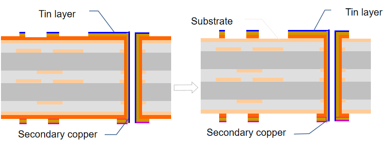
7. Pattern plating
Secondary copper plating: Builds up conductor thickness to customer requirements.
Tin plating: A thin tin layer is added as an etch resist to protect traces during the next step.
8. Etching
Excess copper is chemically etched away, leaving only the tin-protected circuit pattern. Afterward, the tin resist is stripped, exposing the final copper traces.
9. Solder mask
The green (or other color) protective solder mask is applied:
- Pre-treatment: Ensures clean surfaces.
- Solder mask coating: Liquid Photo-Imageable (LPI) solder mask is applied.
- Exposure: UV light hardens the solder mask, leaving pads exposed.
- Development and curing: Non-exposed areas are removed; the mask is baked for durability.
PCB solder masks provide electrical insulation, prevent solder bridging, and improve PCB reliability.
10. Legend (silkscreen)
Component designators, logos, and identifiers are printed using silkscreen or inkjet methods, then baked to ensure adhesion.
11. Surface finish
To protect copper and ensure solderability, finishes are applied:
- ENIG (electroless nickel immersion gold): Excellent for fine-pitch SMT.
- HASL / lead-free HASL: Cost-effective and widely used.
- Immersion tin or OSP: Used for specific applications or cost considerations.
12. Profiling (routing / V-Cut)
The panels are routed, milled, or scored to create individual PCBs in their final dimensions.
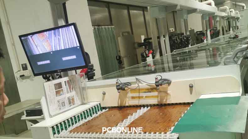
13. Testing
Electrical testing ensures every circuit performs correctly:
- Flying probe testing: Ideal for prototypes and small runs.
- Bed-of-nails testing: Used for high-volume production with test fixtures.
14. Final quality control (FQC)
Before shipment, printed circuit boards undergo:
- Dimensional checks (thickness, hole diameters, spacing).
- Plating checks (thickness, adhesion).
- Surface inspection (solder mask, silkscreen, copper exposure).
- Reliability tests (thermal shock, peel strength, impedance, ionic contamination).
Only PCBs that pass these rigorous inspections move on to PCB assembly or delivery. Below is our video about how PCBs are made by PCBONLINE.
How are Advanced Printed Circuit Boards Made
While the above process applies to most PCBs, some advanced PCBs require additional technologies.
HDI PCBs
HDI (high-density interconnect) PCBs use blind and buried vias to achieve higher wiring density. At PCBONLINE:
- Laser drilling is used to create microvias with micron-level precision.
- Microvias are drilled before lamination, aligning each HDI layer structure.
- Sequential lamination is then performed to build up multiple layers step by step.
- Stacked vias are copper-filled to ensure reliability and conductivity.
The HDI technology is critical for smartphones, tablets, and compact IoT devices where space is limited but performance requirements are high.
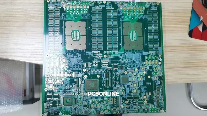
HDI PCB for AI server made by PCBONLINE
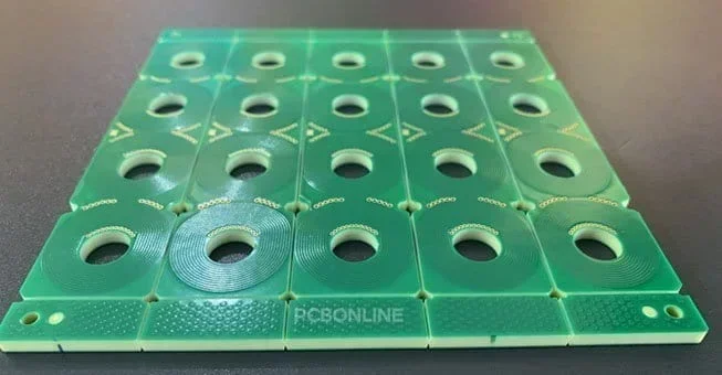
Ceramic PCBs
Ceramic PCBs are used for high-power and high-frequency applications thanks to their excellent thermal conductivity and stability. PCBONLINE manufactures ceramic PCBs using several processes:
- HTCC (high-temperature co-fired ceramic) – Ceramic powder and metal pastes are laminated and sintered at >1600°C.
- LTCC (low-temperature co-fired ceramic) – Glass-ceramic composites are sintered below 900°C, suitable for embedded passive integration.
- DPC (direct plated copper) – Thin copper is directly bonded onto ceramic substrates through sputtering and electroplating.
- Thick-film technology – Conductive and dielectric pastes are screen-printed and fired.
- Thin-film technology – Photolithography is used to create extremely precise and fine features.
ceramic PCBs made by PCBONLINE
Each process has unique advantages. For example, DPC ceramic PCBs offer low thermal resistance and are widely used in high-power LED modules, while LTCC is ideal for RF modules and sensors.
Order Advanced PCB Manufacturing Services from PCBONLINE
If you need one-stop PCB manufacturing from prototyping to mass production, you can partner with PCBONLINE. PCBONLINE is an advanced PCB manufacturer that manufactures and assembles any type of PCBs, including multilayer FR4, HDI, flexible, ceramic, metal-core, and high-frequency.

Founded in 2005, PCBONLINE has two large advanced PCB manufacturing bases, one PCB assembly factory, stable supply chains, and an R&D team for one-stop PCBA manufacturing.
PCBONLINE has strong PCB manufacturing capabilities, including FR4 PCB layers from 1 to 64, high-density PCB, high-frequency PCBs, flexible PCB, rigid-flex PCB, aluminum PCB, copper-based PCB, and ceramic PCB.
PCBONLINE offers free design for manufacturing (DFM) for your PCB and PCBA project, including checking Gerber, bill of materials (BoM), testing files, and solving all technical and unexpected issues during prototyping to ensure the smooth and successful massive production.
PCBONLINE can do the R&D for your PCBA project or take part in your project's development from the early stage for the optimum PCB design and prevent tricky problems in the field application engineering (FAE) stage.
One-stop PCB services meeting your custom needs, including prototyping/sampling, PCB manufacturing, component sourcing, PCB assembly, PCBA value-added, enclosure, and box-build assembly.
High-quality advanced PCB manufacturing certified with ISO 9001:2015, ISO 14001:2015, IATF 16949:2016, RoHS, REACH, UL, and IPC-A-600 Class 2/3.
No matter what applications of your PCB are, like automotive, aerospace, medical devices, IoT, and high-end consumer electronics, PCBONLINE can produce and assemble PCBs that meet the highest performance and reliability standards. To get a quote for your PCB project, contact info@pcbonline.com.
Conclusion
How are printed circuit boards made? The PCB manufacturing process involves laminate preparation, imaging, drilling, plating, solder masking, finishing, and testing. At PCBONLINE, we provide normal PCBs like multilayer FR4 PCBs and metal-core PCBs, and advanced PCBs like HDI and ceramic PCBs. With our turnkey service, strict quality control, and IPC Class 2/3 compliance, PCBONLINE is your trusted PCB partner for medium- to high-end electronic applications.
PCB assembly at PCBONLINE.pdf
PCB fabrication at PCBONLINE.pdf


