
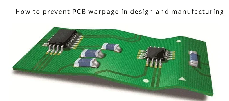
PCB warpage refers to the bending, bowing, and twisting of printed circuit boards. When placing the board on the table which shows at the ends or in the middle of the slightly upward warping, we shall take care because it may impact the quality of overall production and the performance of the PCBA (printed circuit board assembly).
It is critical to reduce the PCB warpage. Here, we reveal the basics of PCB warpage, including the IPC standard of PCB warpage, causes, and how to minimize the warpage.
IPC Standard of PCB Warpage
According to IPC-6012, the identification and performance certification in printed circuit boards, the maximum bow and twist shall be no more than 0.75%; the less, the better.
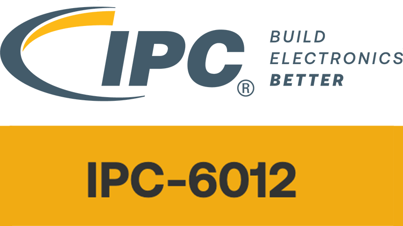
The method to test the PCB warpage follows IPC-TM-650.2.4.22B. It involves putting the board on the calibrated platform, inserting the pin into the point where the curve is largest, and calculating the length of the curved edge of the PCB using the PCB warpage formula.
Warpage= single corner warpage height / PCB diagonal length * 2
Causes of PCB Warpage
The bow and twist of PCBs are mostly due to the stress applied to the board being greater than the stress that the PCB material could withstand. When the board is subjected to uneven resistance, it results in a PCB warpage. In addition, thermal stress, such as overheating during the reflow process, chemical influences, improper production processes, etc., may also cause PCB warpage.
Improper PCB design and manufacturing can both lead to PCB warpage. For example, uneven copper surface area in design and overheating in PCB fabrication can cause warpage.
Uneven copper surface area
The uneven copper surface area on the circuit board will deteriorate the bow and twist of the board. Generally, the Vcc layer is designed with a large area of copper foil. Suppose this area of copper foil cannot be evenly distributed on the board. In that case, it may cause unequal heat absorption and contraction, which leads to different stresses and deformation during manufacturing.
Here are two tips for you:
Utilize copper plating in the hollowed-out area. For example, if the outermost top surface of the board has a larger surface while the bottom has very few, the PCB may have a greater tendency to warp after etching during manufacture.
Meanwhile, try to make the PCB with a balanced layout with a stackup as symmetrical as possible.
Overheating in PCB manufacturing
What's more, if the temperature has reached the upper limit of the Tg value, the PCB will begin to soften, resulting in permanent deformation. For a real case study, a PCB warpage happens when the length of the board is 80mm or more without copper and the thickness of the board is less than 1.0mm.
At the advanced PCB manufacturer PCBONLINE, our engineers has rich experience in setting up the fabrication parameter and our technicians strictly adhere to operating procedures. Overheating can't happen, so you do not worry about that if you work with PCBONLINE.
Design Considerations in Reducing PCB Warpage
In PCB manufacturing, if the rigid PCB is very thin, it can warp. Here are some design considerations for minimizing the PCB warpage.
Increase PCB Thickness
At PCBONLINE, the thickness range of rigid PCBs is from a minimum of 0.12mm (2L) and 0.18mm (4L) to a maximum of 10mm.
A PCB thickness of 1.6 mm is better because it ensures the board does not deform in the reflow oven. If you need a smaller PCB thickness, chat with PCBONLINE from the online chat window. We will give you advice and make some adjustments during our PCB manufacturing to ensure no warpage happens.
Using material in high Tg value
Tg means the glass transition temperature at which the material changes from a glassy state to a rubbery state. The lower the material's Tg value, the faster the FR4 PCB starts to soften when it enters the reflow oven, and the more severe the deformation will be. A high-TG PCB has a smaller deformation during fabrication and assembly.
How do We Prevent PCB Warpage in Manufacturing
PCBONLINE will give its customers a solution for preventing PCB warpages. We can control the PCB warpage within a minimum range. Here are some ways to do it.
Reduce the PCB quantity on the narrow side of the production panel
Reflow ovens use chains to drive the circuit boards forward. The larger the size of the production board, the more possibility of depression deformation will be in the reflow oven. (A production board contains multiple PCBs, and after PCB assembly, it is depanelized.)
The long side of the production panel is placed as a board edge on the chain of the reflow oven. The narrow side of the production panel, therefore, is in the vertical direction of the oven and can be deformed.
For this reason, we need to reduce the number of PCBs on the narrow side of the production panel to minimize the amount of bow deformation.
Use CNC to depanelize PCBs rather than splitting V-cut manually
V-cut is a depanelizing method that creates grooves in the production panel. Basic PCB manufacturers may manually bend the V-cut to split the production panel for PCB depanelization.
However, manually splitting the V-cut can destroy the board's stress structure, leading to a PCB warpage. As an advanced PCB manufacturer, we recommend replacing manually splitting the V-cut with CNC.
There are benefits of depaneling PCB by CNC:
- Not any PCB warpage during depanelization by using CNC
- It eliminates the impact of the stress of manual board splitting on component welding. Manual board breaking will also cause the risk of scrapping the PCBA.
- Smoother appearance and no burrs
- Because the connection with the edge rails is more stable than the half holes, the production panel is flatter during assembly.
We use CNC by default for PCBAs used for middle—and high-end applications, such as automotive, communications, etc. For more details on PCB fabrication, please get in touch with us. We shall tell you the most suitable panelization and depanelization method for your PCB design.
Bake PCBs before Electronic Assembly
The purpose of baking PCBs before discharging is to remove the moisture in the PCB board. At the same time, make the resin in the laminate fully cured and further eliminate the residual stress in the laminate, which is helpful in preventing the PCB from warping.
Below, you can see how PCBONLINE bakes various types of PCBs, components, and printed circuit board assemblies (PCBAs).
|
Materials to be baked
|
Package materials
|
Baking temperatures
|
Temperature setting
|
Baking time
|
||
Package thickness |
Moisture sensitivity level |
Baking time |
||||
|
Components
|
With a tray: Confirm that the tray can withstand temperatures of 125 degrees or above.
|
110+/-5
℃
|
110℃
|
≤1.4mm
|
2, 2A, 3 |
8 hours |
≤1.4mm |
4, 5, 5a |
16 hours |
||||
≤2.0mm |
2, 2A, 3 |
24 hours |
||||
|
Bulk materials need to be placed in high-temperature resistant trays
|
≤2.0mm |
4 |
32 hours |
|||
≤2.0mm |
5 |
40 hours |
||||
≤2.0mm |
5a |
48 hours |
||||
|
Components in tubes
|
45+/-5
℃
|
45℃
|
48+/-1 hours |
|||
|
Components in tapes and reels
|
||||||
|
Blank PCB
|
HASL and immersion gold PCBs
|
100-120
℃
|
100
℃
|
4+/-1 hours
|
||
|
75+/-5
℃
|
75
℃
|
12+/-1 hours
|
||||
|
OSP, immersion silver, and immersion tin PCBs cannot be baked. If PCBs are not in their original packaging or have been stored in the original packaging for more than 3 months, return them to the PCB factory for rework.
|
||||||
|
PCBA
|
With only SMDs without PTH parts (WI-FI, Bluetooth, 4G modules, etc.)
|
100-120
℃
|
100
℃
|
4+/-1 hours
|
||
|
75+/-5
℃
|
75
℃
|
12+/-1 hours
|
||||
|
With PTH parts (but if there's a display screen, the board cannot be baked)
|
75+/-5
℃
|
75
℃
|
12+/-1 hours
|
|||
|
cleaned PCBA
|
75+/-5
℃
|
75
℃
|
14+/-1 hours
|
|||
|
Flexible PCB
|
Baking tray
|
100+/-5
℃
|
100
℃
|
1-2 hours
|
||
|
PCBA with LED
|
LED beads have special requirements and need to be baked according to the requirements on the LED packaging.
|
|||||
How do PCB Manufacturers Handle PCB Warpage
First, I need to tell you that PCBONLINE's PCB and PCBA have no warpage. Dealing with PCB warpage leads to additional costs and time to rework, which is unnecessary and can be avoided.
During PCB manufacturing, the PCB boards are checked for 100% flatness during our final inspection. Boards with warpages will be picked out and leveled by a roll leveler.
During PCB assembly, if the PCB warpage happens after reflow soldering, the 3D automated optical inspection (AOI) will check it out.
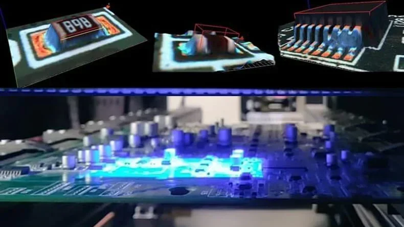
All unqualified boards will be picked out and put into the oven at 150 degrees Celsius, where they will be baked for 3 to 6 hours under heavy pressure to restore their flatness. Later, they will be cooled down under heavy pressure. A few boards may still need to undergo two to three times of pressure to reach satisfied flatness. Since the AOI inspection step, all these reworked boards are separate from those all-goods ones.
Hassle-free Work with High-quality PCB Fabricator and Assembler
PCB warpage is an annoying hassle. Though it can be fixed by leveling, it may come back during device use. We all don't expect the PCB warpage to happen. Thus, you can work with a high-quality PCB fabricator and assembler, PCBONLINE, to ensure the best performance of your devices without quality hassle.
PCBONLINE is a one-stop PCBA manufacturer founded in 1999. It has two large advanced PCB manufacturing bases, one EMS (electronic manufacturing service) PCB assembly factory, and an R&D team to provide engineering support and solve technical issues.
PCBONLINE is a source factory manufacturer for one-stop electronics manufacturing covering PCB fabrication, component sourcing, PCB assembly, PCBA value-added, and box-build assembly.
Our PCB fabrication follows IPC-A-600 Class2/3 for middle and high-end applications without PCB warpage issues.
PCB and PCBA manufacturing at PCBONLINE is certified with ISO 9001:2015, IATF 16949, RoHS, REACH, IPC, and UL.
Traceable materials and electronic manufacturing, rigorous operation procedures, and comprehensive testing ensure hassle-free.
Our engineers have an average of 20 years of experience in engineering, R&D, and solving technical issues.
We will do a DFM (design for manufacturing) for your project for free and optimize your design, which can reduce your fabrication costs without function or quality sacrifice.
Once you receive a quote from us, we will follow up on your project with one-on-one support. For one-stop PCB and electronics manufacturing, please email PCBONLINE at info@pcbonline.com.
Conclusion
In this article, we have discussed how to minimize PCB warpage. Mutual communication between you and your PCB manufacturer is important to produce top-quality PCB boards and electronic devices. PCBONLINE is always here for you and will offer professional solutions. Contact us by email or online chat today!
PCB fabrication at PCBONLINE.pdf


