
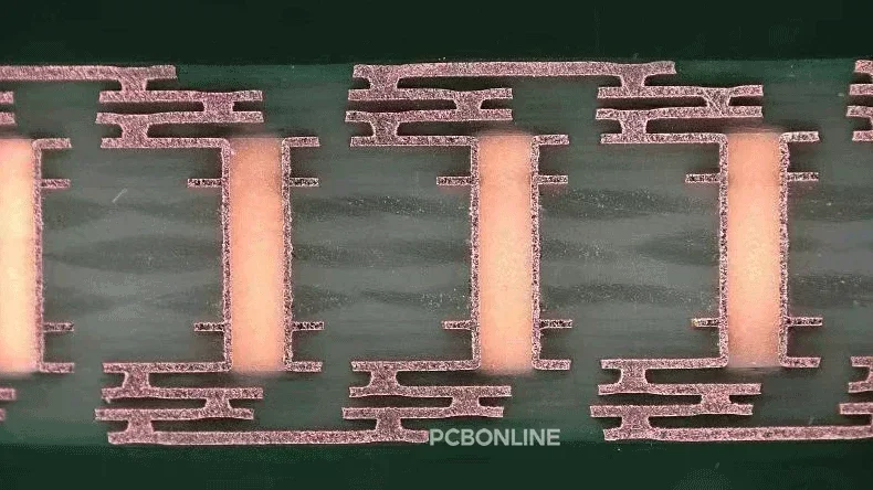
HDI is high-density-interconnected, and an HDI PCB is a printed circuit board featuring microvias, blind and buried holes, small line width/space, and fine-pitch components. Besides, the HDI PCB manufacturing process requires sequential lamination to make the board structures of 1+N+1, 2+N+2, 3+N+3, 4+N+4, and even more.
Do you have any clues for the HDI PCB design? What are a PCB manufacturer's HDI PCB manufacturing capabilities? This blog shows the HDI PCB capabilities of an HDI PCB manufacturer, PCBONLINE. You can see the 4-layer HDI PCB's impedance control and lamination structure designs for reference.
HDI PCB Manufacturing Capabilities from PCBONLINE
The table below shows the minimum parameter limits we can make in HDI PCB manufacturing:
|
HDI PCB parameters
|
Manufacturing Capabilities at PCBONLINE
|
|
Minimum mechanical hole aperture
|
0.2mm
|
|
Minimum laser hole aperture
|
0.1mm
|
|
Minimum line width and line spacing
|
3/3mil, normal capability is 4/4mil
|
|
Minimum pad to pad
|
3mil, normal capability is 4mil
|
|
Minimum pad to line
|
3mil, normal capability is 4mil
|
|
Minimum VIA AR
|
5mil, normal capability is 6-8mil
|
|
Minimum PTH AR
|
8mil, normal capability is 10mil
|
|
Minimum hole center to hole center
|
8mil, normal capacity is 10mil
|
Here are some explanations of the HDI PCB manufacturing process so that you can easily understand the above table. In an HDI PCB, the core layers are first manufactured, whose holes are through-holes (PTH) that are mechanically drilled. After the core is laminated and plated, the outer layers are laminated and plated on the core cycle-by-cycle, whose holes are microvias that are laser drilled. Each cycle creates an outer layer above and below the core.
4-layer HDI PCB Impedance Design
Impedance control is a vital consideration in HDI PCB design. Here are two impedance designs for a 4-layer 1.6mm-thick HDI PCB for reference.
Impedance design 1 for 4-layer 1.6mm-thick HDI PCB (board thickness tolerance: +/-0.16mm)
|
Layer
|
Impedance properties
|
Line width MIL
|
Line spacing MIL
|
Copper spacing
|
Copper thickness (finished product) OZ
|
Recommended impedance value OHM
|
Reference layer
|
Impedance value tolerance range
|
|
L1
|
characteristic
|
5
|
1
|
50
|
L2
|
+/-10%
|
||
|
L4
|
characteristic
|
5
|
1
|
50
|
L3
|
+/-10%
|
||
|
L1
|
difference
|
4.5
|
7
|
1
|
100
|
L2
|
+/-10%
|
|
|
L4
|
difference
|
4.5
|
7
|
1
|
100
|
L3
|
+/-10%
|
Impedance design 2 for 4-layer 1.6mm-thick HDI PCB (board thickness tolerance: +/-0.16mm)
|
Layer
|
Impedance properties
|
Line width MIL
|
Line spacing MIL
|
Copper spacing
|
Copper thickness (finished product) OZ
|
Recommended impedance value OHM
|
Reference layer
|
Impedance value tolerance range
|
|
L1
|
characteristic
|
9
|
1
|
50
|
L2
|
+/-10%
|
||
|
L4
|
characteristic
|
9
|
1
|
50
|
L3
|
+/-10%
|
||
|
L1
|
difference
|
6
|
5
|
1
|
100
|
L2
|
+/-10%
|
|
|
L4
|
difference
|
6
|
5
|
1
|
100
|
L3
|
+/-10%
|
The above two impedance control designs are for 4-layer PCBs. To learn about impedance control for HDI PCBs with more layers, please contact PCBONLINE. (You can talk with us from the online chat window now.)
4-layer HDI PCB Stack-up/Structure Design
There are two 4-layer HDI PCB stack-up or structure designs corresponding to the above two impedance control designs.
Stack-up/structure design 1 for 4-layer 1.6mm-thick HDI PCB (board thickness tolerance: +/-0.16mm)
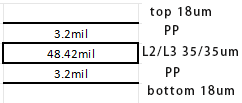
|
Layer
|
Thickness
|
ER
|
|
Top layer copper
|
18um
|
/
|
|
PP
|
3.2mil
|
4.2
|
|
L2/L3 copper
|
35/35um
|
4.2
|
|
PP
|
3.2mil
|
4.2
|
|
Bottom layer copper
|
18um
|
/
|
Stack-up/structure design 2 for 4-layer 1.6mm-thick HDI PCB (board thickness tolerance: +/-0.16mm)
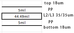
|
Layer
|
Thickness
|
ER
|
|
Top layer copper
|
18um
|
/
|
|
PP
|
5mil
|
4.2
|
|
L2/L3 copper
|
35/35um
|
4.2
|
|
PP
|
5mil
|
4.2
|
|
Bottom layer copper
|
18um
|
/
|
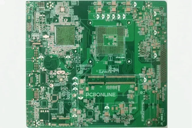
One-Stop HDI PCB Manufacturer PCBONLINE
PCBONLINE is a one-stop electronics manufacturer providing 4-to-64-layer HDI PCB fabrication, assembly, and PCBA box-build assembly. HDI PCBs can be manufactured in various substrate materials and types, such as FR4, polyimide (flexible PCB), polyimide + FR4 (rigid-flex PCB), aluminum, ceramics, and copper.

3000 m² of production capacity per day for HDI PCBs with builds of 1+N+1, 2+N+2, 3+N+3,4+N+4, and arbitrary interconnection in any layers.
PCBONLINE offers an extensive range of technologies and solutions that meet the highest requirements.
We can manufacture complex HDI PCBs, inlay boards, heavy copper designs, and hybrid and fine structure lay-ups.
Besides HDI PCB fabrication, we have powerful capabilities in fine-pitch assembly for HDI PCB assembly.
We have rich R&D and manufacturing experience for HDI PCB applications such as FPGA boards. High-quality HDI PCB and PCBA manufacturing certified with ISO 9001:2015, IATF 16949, RoHS, REACH, UL, and IPC-A-610 Class 2/3.
If you need HDI PCBs or technical support for your HDI PCB/product design plan, please send your email to PCBONLINE at info@pcbonline.com. We will follow up with you and provide one-on-one help and service to you.
Conclusion
This blog provides two HDI PCB designs regarding impedance control and stack-up. Both work for a 4-layer HDI PCB with a 1.6mm thickness. To learn more about HDI PCB capabilities and designs, please chat with PCBONLINE to get the solution that meets your custom needs.
PCB fabrication at PCBONLINE.pdf


