High-density PCBs have transformed the electronics industry by diminishing the size and weight of electronic gadgets while upgrading their usefulness. Let's explore high-density PCBs in this blog post!
Part 1. High-Density PCB
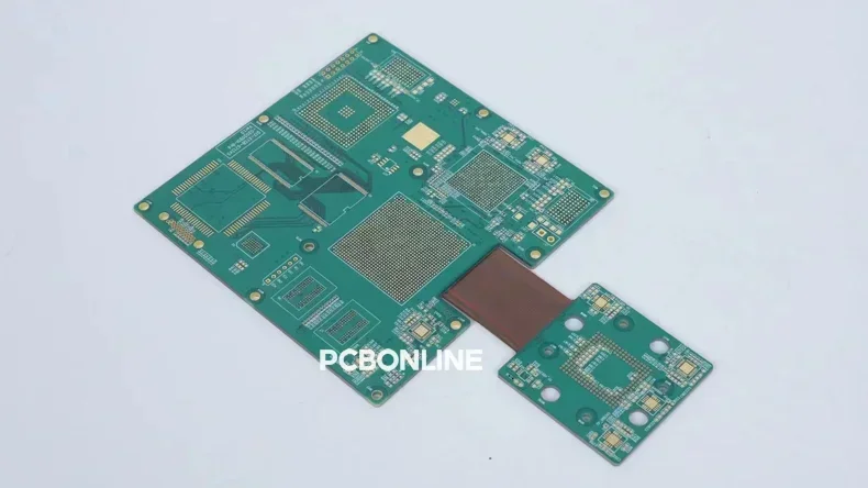
High-density PCB or high-density interconnect (HDI PCB), is an important development in the world of printed circuit boards.
High-density PCBs are designed with a focus on maximizing the density of components and interconnections in a smaller footprint.
High-density PCB is accomplished by using cutting-edge methods and technologies including buried vias, blind vias, and micro vias.
Microvias make it possible to create PCBs that are highly sophisticated and tiny, making them ideal for high-performance electronics like cell phones, tablets, and high-level clinical devices.
As high-density PCB uses micro vias, they are also called micro via PCB.
As technological innovation continues to accelerate, high-density PCBs will play a crucial role in enabling the development of smaller, more powerful, and environmentally friendly electronic devices.
Part 2. High-Density Interconnects Stack-up
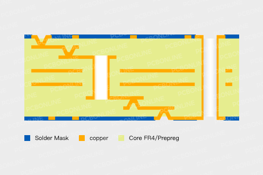
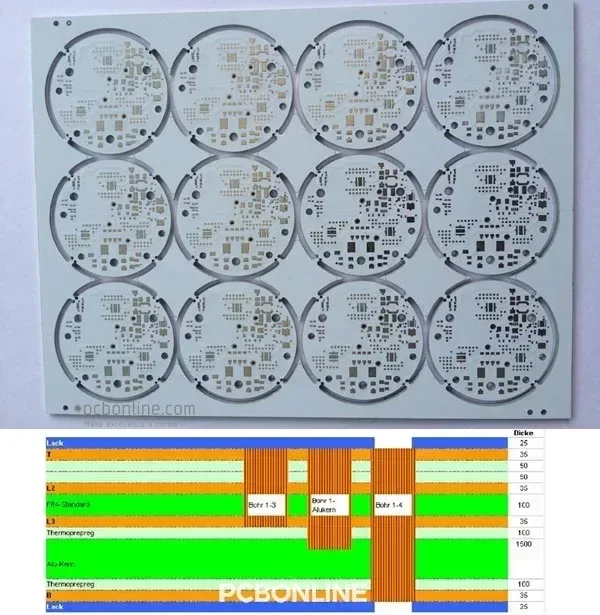
High-density stack-up refers to the arrangement of multiple layers of circuitry in a three-dimensional structure, allowing for a significant increase in component density and performance within a smaller footprint.
High-density stack-up involves the arrangement of multiple PCB layers to accommodate a complex network of electronic components and connections efficiently.
Here's a simple explanation:
In a high-density stack-up, PCB designers use multiple layers of circuit boards stacked on top of each other. Each layer has its own set of electrical pathways called traces, which carry signals and power to different parts of the device. By stacking these layers, you can fit more components and connections into a smaller space, making your electronic device compact and powerful.
The number of layers and how they are arranged in a high-density stack-up depends on the complexity of the electronic device. For instance, a smartphone may have many layers, each serving a specific purpose. Some layers might be dedicated to power distribution, while others handle data signals.
Designers carefully plan the stack-up to minimize interference between the different traces and ensure efficient signal flow.
High-density stack-up is crucial for achieving performance and functionality. It allows engineers to create compact and feature-rich devices while maintaining signal integrity and reducing electromagnetic interference. This technique is at the heart of many advanced electronic products we use every day, making them faster, more capable, and packed with technology.
Part 3. Features of High-Density PCB
Here are some features of high-density PCB.
High-speed signal integrity
High-speed signal integrity is paramount in contemporary electronics in telecommunications and digital systems. Ensuring signal integrity at elevated frequencies demands meticulous management of impedance matching, reduction of electromagnetic interference, and precise control of signal reflections.
Design complexity
Conventional PCBs are typically single-layer or double-layer boards with relatively simple designs. They are frequently utilized in basic electronic devices whose circuitry is straightforward and does not require extensive integration.
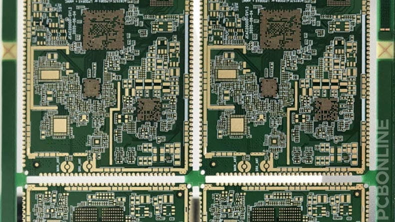
In contrast, high-density PCBs, are designed to accommodate complex and densely packed circuits. They often have multiple layers enabling a much higher component density.
Manufacturing techniques
Normal PCBs are manufactured using traditional methods like through-hole plating for vias and relatively simple automated assembly processes.
On the other hand, high-density PCBs demand more complex sequential lamination. Precision is required when working with sophisticated materials, and techniques like controlled impedance and laser drilling are frequently used.
Part 4. Applications of High-Density PCB
Conventional PCBs are commonly used in simpler electronic devices like toys, household appliances, and basic industrial equipment. They are excellent for goods where complex functionality is not a top priority because of their simplicity and affordability.
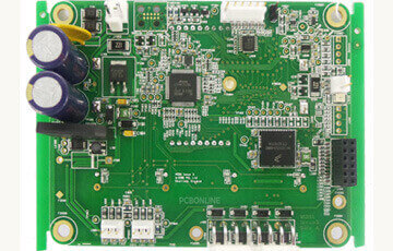
In contrast, high-density PCBs are integral to cutting-edge technology. They are used in devices that require high-speed data transmission, miniaturization, and advanced functionality, such as FPGA boards, high-performance computers, and automotive radar systems.
Part 5. Manufacturing of High-Density PCB
A high-density PCB project involves PCB design, PCB fabrication, and PCB assembly.
Design and layout
The process begins with the design and layout of the PCB. Engineers carefully plan the arrangement of components, traces, and layers to maximize efficiency and minimize space usage. Special attention is given to the placement of high-density components such as microprocessors, memory chips, and connectors.
Component placement and routing considerations
The thoughtful placement of heat-generating elements is imperative for effective thermal management.
In parallel, the proximity of decoupling capacitors to high-speed component power pins is crucial to maintain a stable power supply and mitigate noise.
On the routing front, preserving signal integrity is paramount.
Controlled impedance routing guidelines are followed for high-frequency traces, safeguarding against signal reflections.
Design rule checks and verification
Design rule checks (DRC) and verification play a pivotal role in ensuring the accuracy, functionality, and manufacturability of high-density PCB designs.
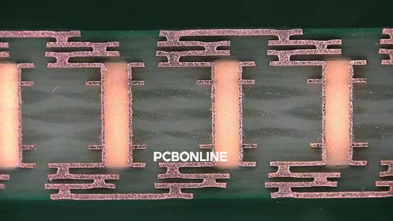
PCB vias such as micro vias and blind vias, common in high-density layouts, require precise verification to ensure that they meet both electrical and manufacturability constraints.
By conducting comprehensive DRC and verification, designers can identify and rectify design errors early in the process, reducing the likelihood of costly rework or manufacturing delays.
This process ensures that the final high-density PCB design not only meets performance requirements but is also manufacturable within the chosen fabrication technology's capabilities.
Fabrication of high-density PCB
The manufacturing of high-density PCBs relies on several advanced technologies.
Laser drilling. High-density PCBs often incorporate microvias, which are extremely small holes that connect different layers of the board. Laser drilling allows for the precise and efficient creation of these microvias.
Sequential lamination. High-density PCBs frequently contain numerous layers and complex connections between them. The precise alignment and bonding of these layers are achieved through advanced lamination processes. To ensure uniform bonding and avoid problems like delamination, controlled pressure, and temperature profiles are controlled.
Quality assurance and testing
Quality assurance is paramount in high-density PCB assembly. Automated optical inspection (AOI) and X-ray inspection systems are used to detect defects like misalignment, soldering issues, and component placement errors. In-circuit testing (ICT) and functional testing validate the functionality of the assembled boards.
Rigorous testing ensures that the final product meets the highest quality and reliability standards, crucial in industries where failure is not an option.
Part 6. One-Stop Through-Hole PCB Assembly Manufacturer
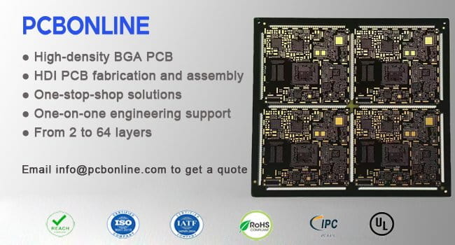
PCBONLINE provides one-step solutions to get your high-density PCBs fabricated.
Founded in 1999, PCBONLINE has 3000m² of high-density PCB production capability per day.
At PCBONLINE, precise and controlled mechanical deep drilling rounds off the technical possibilities for high-density.
PCBONLINE provides high-density PCB EMS solutions from the initial idea to high-volume production.
PCBONLINE meets every technical requirement for your project with top cost-effectiveness.
PCBONLINE has rich high-density PCB experiences for applications, including battery switches, power distributors, motor controls, LEDs, controls, automotive, satellites, microsystems, and communication electronics.
You can check part of the high-density PCB fabrication capabilities at PCBONLINE:
- High-density PCB layer quantity: 4 to 64
- Maximum high-density layer quantity: 20
- High-density builds: 1+N+1, 2+N+2, 3+N+3, 4+N+4, any layer in R&D
- Micro via: single micro vias, staggered vias, stacked vias, and skipped vias
- Minimum laser drill: 0.075mm
- Minimum mechanical drill: 0.15mm
- High-density PCB types: inlay boards, heavy-copper boards, hybrid and fine structure lay-ups, FR4, MCPCB
Ordering high-density PCBs from PCBONLINE is buying quality that pays for itself over time. If you need high-density PCB fabrication and assembly, feel free to contact PCBONLINE by email at info@pcbonline.com.
Conclusion
High-density PCBs are well-positioned to be the preferred choice for the future of electronics due to their ability to support miniaturization, high-speed data transmission, advanced functionality, and more sustainable manufacturing practices. PCBONLINE is a one-stop high-density PCB manufacturer with the best cost-effectiveness. You can chat with us from the chat window on the right.
12-Layer HDI PCB Structure Reference.pdf