
Graphics Processing Unit (GPU) parallels data processing for AI, machine learning, and high-performance computing. The immense power and high-frequency operations of a GPU bring significant challenges to the platform that houses it, the HDI Printed Circuit PCB (PCB). The GPU PCB must meet extreme demands for high-density interconnects (HDI), signal integrity, thermal management, and high-frequency demands.
The turnkey advanced PCB manufacturer PCBONLINE provides robust manufacturing and assembly for GPU PCBs. In this article, we explore how a GPU PCB makes a perfect balance of HDI, electromagnetic compatibility (EMC), and thermal dissipation, and how we ensure the successful manufacturing and assembly of GPU PCBs.
Part 1: GPU vs. CPU vs. FPGA
GPU is specialized for AI parallel processing. On a PCB, a GPU chip is in the ball-grid array (BGA) package to surface mount on the printed circuit PCB. To understand why AI relies on GPU rather than other chips, it's helpful to compare it to other processors, CPU and FPGA.
- Graphics Processing Unit (GPU): The GPU is massive and highly efficient. It has thousands of smaller cores designed for parallel processing. This makes it ideal for AI training and data science, as its architecture is perfectly suited for crunching vast datasets.
- Central Processing Unit (CPU): A CPU is good at sequential tasks and complex decision-making. With a few powerful cores, it handles the operating system and most general applications. However, it's inefficient for the massive parallel tasks required by AI.
- Field-Programmable Gate Array (FPGA): An FPGA is versatile and custom-built and can be reconfigured for any task. It's used for applications requiring extremely low latency. While highly efficient for specific workloads, it's generally more complex to program and less flexible than a GPU for the broad demands of AI.
|
Feature
|
CPU
|
GPU
|
FPGA
|
|
Primary task
|
Sequential processing
|
Parallel processing
|
Reconfigurable logic
|
|
Number of cores
|
Few (e.g., 8-32)
|
Thousands
|
N/A (Logic blocks)
|
|
Best for
|
General computing, OS
|
AI/ML, graphics
|
Specialized hardware
|
Part 2: Introduction to the GPU PCB
The GPU PCB is the electronic platform that connects the GPU to other components, such as high-bandwidth memory (HBM), the motherboard (via PCIe), and the power delivery system.
At PCBONLINE, our GPU PCBs provide a stable, low-noise environment for the GPU to operate at peak performance and ensure robust power and signal integrity.
Compared with other PCBs, a GPU PCB presents these features:
- A high layer count of at least 24 layers and high-density interconnect
- Handling extreme data rates and high frequencies
- Managing significant power consumption and heat generation
- The need for a perfect balance between thermal management and signal integrity
Part 3: GPU PCBs Are 24+ Layer HDI
A 24+ layer count is necessary for a GPU PCB because thousands of pins of the GPU require multiple layers for routing high-speed signals and power, and ground planes.
- In a GPU PCB, high-speed signals transfer between the GPU and video memory (such as HBM) and the PCIe interface. They must be routed on individual inner layers with strict impedance control.
- And each high-speed inner layer must be between two ground layers to suppress noise.
- Power planes provide a stable power supply so that the GPU can deal with parallel processing that needs significant power. Ground planes maintain signal integrity and EMC. Here, power and ground planes typically have a larger copper thick copper layers, which also conduct heat efficiently from the GPU chip.
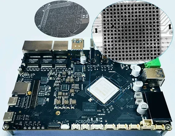
A GPU has a large number of pins. To connect these pins to other components, PCBs must use high-density interconnect (HDI) technology, such as blind and buried vias for routing signals under the dense BGA pad of the GPU. These multi-stage blind/buried vias create complex circuits within a limited space.
At PCBONLINE, microvias that penetrate only one circuit layer in these HDI PCB layers are pre-drilled by laser and plated on each sub-stack. Then we use sequential lamination to build the HDI structure, blind and buried vias, of the GPU PCB.
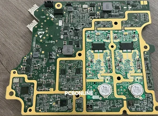
GPU server PCB manufactured by PCBONLINE
Part 4: GPU PCBs Maintain Signal Integrity at High Frequencies
GPUs operate at high frequencies. As signals can easily degrade because of attenuation, reflection, and crosstalk, a GPU PCB design must maintain signal integrity.
To maintain signal integrity, a GPU PCB uses high-frequency PCB materials of low Dk (dielectric constant) and low Df (dissipation factor) to minimize signal loss, such as low-DK FR4, PTFE, and ceramics.
A GPU PCB also implements controlled impedance traces to prevent signal reflections.
In a GPU PCB design, high-speed signal trace widths are consistent, high-speed signal spacing is at least 3 times the trace width, and the dielectric thickness is thin.
Furthermore, high-speed differential pairs (for connections like PCIe and HBM) are routed in inner layers, sandwiched between ground planes to provide natural shielding and prevent crosstalk.
Part 5: GPU PCBs Balance Heat Dissipation and EMC
A GPU chip consumes a high amount of power, hundreds of watts. It generates a lot of heat, so the GPU PCB must dissipate heat efficiently for long-term reliability.
For stable operation, a GPU PCB should have a good heat dissipation design, using:
- thick-copper PCB layers
- inlaid copper busbars
- heat sinks
- and a fan to assist in heat dissipation
However, thick copper layers, copper busbars, and heat sinks may affect EMC, as a large area of metal, if not designed properly, can become an antenna and radiate electromagnetic waves. How do GPU PCBs deal with the natural conflict between thermal dissipation and EMC or signal integrity?
- High-speed signal areas, power supply areas, and heat dissipation areas are carefully planned and separated. Fine traces fanned out from the GPU BGA are placed on inner layers of the PCB to achieve optimal signal integrity and shielding.
- Thick copper layers, often used as power or ground planes, act as effective electromagnetic shields. As long as these layers remain intact and well-grounded, they effectively suppress electromagnetic interference rather than radiate it.
- Maintain a safe distance between large heat sinks, such as busbars and heat sinks, and the GPU area to not interference with the high-speed signal area. Furthermore, the heat sink's mounting bracket and grounding connections must be carefully designed to ensure they do not become sources of electromagnetic radiation.
- Besides, the multilayer PCB inherently provides strong EMI suppression capabilities. By sandwiching high-speed signal traces between two ground planes, a microstrip or stripline structure is formed, effectively confining electromagnetic fields around the traces and preventing them from radiating outward.
Part 6: GPU PCB Manufacturing and Assembly
What's special about GPU PCB manufacturing? It requires:
- Precision microwave laser drilling and positioning
- Sequential lamination
- Copper thickness testing
- Plasma treatment
- Thermal shock testing
Since GPU PCBs are all HDI PCBs with more than 24 layers, sequential lamination is required for the layers with pre-laser drilled microvias, and the layers are stacked or staggered one by one precisely to build the desired blind and buried multilayer holes.
Due to the high impedance control requirements, the copper thickness must be tested. We strictly control the parameters during the electroplating process and use X-ray fluorescence and micro-sectioning methods to ensure that the copper thickness meets the design requirements.
Since the PCB works at high frequencies, Plasma treatment is also required to ensure that the copper traces and copper hole walls are free of any bubbles or dirt after lamination.

Thermal shock testing is also required to ensure that there is no delamination of the hole walls.
What's special about GPU PCB assembly?
During assembly, we must provide fine-pitch assembly capabilities, preferably a 0.4mm patch. For THT assembly of through-hole components such as heat sinks and PCIe interfaces, we must design our wave soldering fixture to avoid component lifting or offsetting during the wave soldering process, due to the component pin being too long or the component being lightweight.
Besides, as GPUs are large-size BGA chips, GPU PCB assembly requires a specialized reflow profile and temperature control to prevent BGA warpage and 100% X-ray inspection to ensure the voiding rate is under 10%. At PCBONLINE, we usually control the BGA voiding rate below 5% and can even control it under 3.5%.
Also, if you use second-hand GPUs for your PCB, the GPUs require reballing and 125℃ baking @ 24 hours before GPU PCB assembly. PCBONLINE will handle all the GPU PCB manufacturing and assembly for your project under one roof.
Part 7. Partner with PCBONLINE for GPU PCBs
PCBONLINE has rich experience in GPU PCB manufacturing and assembly. We have delivered successful GPU PCB projects for top-tier companies.

Founded in 2005, PBONLINE has two large advanced PCB manufacturing bases and one PCB assembly factory.
We are an advanced PCB manufacturer for HDI, high-frequency, and high-thermal-conductivity PCBs, exactly meeting the GPU PCB manufacturing demands.
From GPU PCB manufacturing and assembly to GPU BGA reballing and programming, we handle your project under one roof, protecting your intellectual property and saving time and costs.
PCBONLINE has complete testing and reballing equipment for BGA GPU reballing, from chip functionality inspections to reballing, GPU PCB assembly, X-ray inspection for BGA voiding <5%, and GPU reprogramming.
Our HDI GPU capabilities allow blind, buried, staggered, and stacked vias and arbitarily connected HDI structure layers from 4 to 64 layers.
We take care of all details such as PCBA fixture design, reflow and wave oven temperature control, and production process design, to ensure the success of your GPU PCB project.
High-quality GPU PCBA manufacturing certified with ISO 9001:2015, ISO 14001:2015, IATF 16949:2016, RoHS, REACH, UL, and IPC-A-610 Class 2/3.
PCBONLINE will ensure the success of your project and solve all issues with one-on-one engineering support throughout your GPU PCB project.
PCBONLINE will check your Gerber carefully to make sure your GPU PCB design is feasible and help solve technical issues. If you feel interested in GPU PCB/PCBA from PCBONLINE, send your inquiry by email to info@pcbonline.com.
Conclusion
GPU PCBs are 24+ layer HDI PCBs operating at high frequencies and power requirements. They need to address HDI, EMI, and high-thermal dissipation challenges simultaneously. If you need high-voltage PCB manufacturing and assembly, contact PCBONLINE to start your project with confidence.
©This article is an original work of the PCBONLINE team. Please indicate the author PCBONLINE if you reprint. If the article is reproduced without permission or without indicating the author's source, PCBONLINE reserves the right to investigate the infringement.
Battery Management System Manufacturing at PCBONLINE.pdf
CCS Product Introduction - PCBONLINE.pdf


