
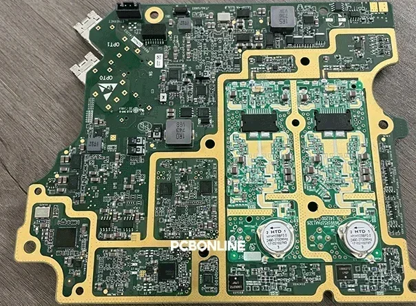
Graphics Processing Units (GPUs) are flip-chip ball-grid-array (BGA) chips, dealing with parallel processing for GPU AI servers and AI high-performance computing. To have the GPU work properly, you will need PCB assembly services to surface mount it onto a printed circuit board (PCB).
GPU PCB assembly demands extreme reliability. GPU PCBs must handle high-density-interconnect (HDI), high frequency, and high power consumption. So, GPU PCB assembly must deal with fine-pitch assembly for BGA, temperature control in case of warpage, and voiding rate controlled within 5%.
PCBONLINE is a one-stop HDI and high-frequency PCB manufacturer, providing GPU PCB manufacturing and assembly, including design for manufacturing (DFM) and BGA reballing for refurbished GPUs if needed. In this article, we'll explore the main challenges in GPU PCB assembly, focusing on BGA voiding rate control, reflow soldering, and reliability verification.
Part 1: Why GPU PCB Assembly Is More Complex Than FR4 PCB Assembly
GPU PCB assembly is one of the most demanding processes in electronics manufacturing.
Unlike general-purpose PCBs, a GPU PCB features fine-pitch BGA packages, multi-layer HDI design, high-speed signal integrity, and strict thermal reliability requirements.
GPU-based equipment is power-hungry, heat-intensive, and signal-sensitive systems that run at high frequencies. These requirements introduce challenges in turnkey GPU PCB assembly across:
- PCB DFM – usually 24+ layers with HDI PCB microwave structures.
- Component mounting – large fine-pitch GPU in the BGA package, video random access memory (VRAM), high-speed controllers, and other components like resistors and inductors.
- Soldering process – precise thermal profiles for thousands of solder joints in reflow soldering.
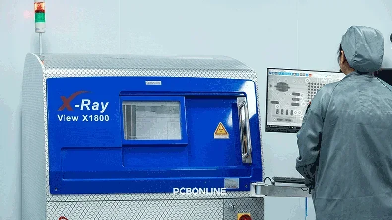
- Reliability requirements – long-term stability under constant high-power workloads. The BGA hidden joints need an X-ray inspection to ensure solderability.
For these reasons, SMT lines for GPU PCB assembly must offer fine-pitch capabilities (GPU pitch: 0.5mm - 0.6mm, and fine-pitch means 0.65mm and below) for BGA and be equipped with an X-ray machine. PCBONLINE's OEM PCB assembly factory meets GPU PCB assembly requirements, and we have rich experience in process design and wave temperature control to ensure the success of GPU PCB assembly and the final devices.
Part 2. Fine-Pitch BGA Soldering Accuracy and Baking
One of the greatest challenges in GPU PCB assembly is BGA placement.
- A GPU is a large BGA, containing thousands of solder balls, with a pitch ranging from 0.4 mm to 0.8 mm.
- The placement tolerance must be extremely tight. Any slight misalignment can cause bridging (short circuits) or open joints.
- Solder paste printing, stencil thickness, and pick-and-place accuracy are all important in GPU PCB assembly.
At PCBONLINE, our automatic SMT lines use high-precision printers and advanced placement machines (2 YAMAHA YSM20R machines + 1 YSM10 machine) to handle fine-pitch BGAs. Combined with SMT stencil design optimization, we ensure that every solder joint is positioned with perfect alignment.
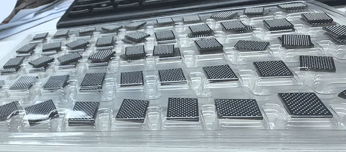
Besides, if your GPU is not factory-new, sealed, dry-packed, and within the moisture sensitivity level (MSL) exposure time, we take care of GPU baking to prevent the BGA popcorn effect. GPUs are generally MSL 3, thickness ≥2mm, so we will bake the refurbished GPU after BGA reballing at 125°C for 24 hours.
Part 3: Large BGA Warpage Control for GPU PCB Assembly
Unlike small ICs, a GPU BGA package can measure 20 × 20 mm to 40 × 40 mm or even larger. During reflow soldering, the GPUs are prone to warpage due to thermal stress without proper oven temperature control.
The risks of BGA warpage lie in: If the package bends upward, edge balls may not connect properly. If it bends downward, center balls may float, creating hidden openings.
To minimize GPU warpage in GPU PCB assembly, PCBONLINE uses:
- Optimized lead-free reflow temperature profiles with balanced preheat, soak, and peak stages.
- PCB techniques such as via-in-pad with copper filling to enhance flatness.
- Process simulation and inspection to prevent joint failures caused by deformation.
Part 4: Thermal Management in GPU PCB Assembly
GPUs consume power from tens to hundreds of watts, producing much heat during operation. The GPU PCB must manage heat efficiently both during assembly and throughout its service life.
During reflow, we control the soldering oven temperatures for uniform heating to avoid thermal gradients that lead to stress cracks.
In operation, the GPU PCB needs thick copper planes, thermal vias, and an optimized stackup to dissipate heat effectively. Our engineers will check all the thermal paths to ensure the thermal dissipation of the GPU PCBA during our DFM.
During the GPU PCB assembly project, our engineers will collaborate closely with your engineering team to ensure your design with enhanced thermal performance.
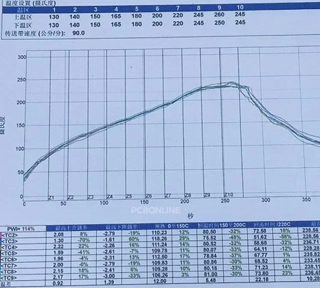
Besides, our reflow soldering ovens are lead-free and programmable with 10 temperature zones, meeting the GPU temperature control requirements. PCBONLINE ensures reliable soldering and stable long-term operation.
![]()
Part 5: Reflow Soldering Precision in GPU PCB Assembly
Some engineers mistakenly believe that GPU PCBs require higher reflow temperatures. In reality, the challenge lies in precise control of the reflow curve, not excessive heat.
With lead-free solder (SAC305), the peak temperature is 240–250 °C.
The key to reflow soldering in GPU PCB assembly is to strictly control the ramp-up and ramp-down rate to prevent thermal shock, warpage, and solder defects.
During the process design, the PCBA engineers at PCBONLINE will provide a properly profiled reflow curve. It ensures that all solder balls melt and wet evenly, without damaging the GPU BGA package or PCB.
PCBONLINE applies customized reflow profiles for GPU assemblies, based on PCB size, component density, and thermal mass, ensuring consistent high-quality results.
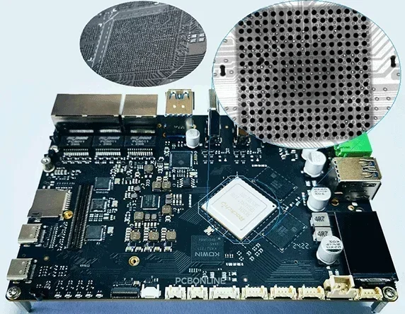
Part 6: X-Ray Inspection and Voiding Control
Since all GPU BGA solder joints are hidden under the package, automated optical inspection (AOI) is impossible for their solder balls. Instead, we use the X-ray inspection to check the AOI solder joints after reflow soldering.
Voiding, trapped air pockets inside solder joints, is a major concern, especially for high-power GPUs. During soldering, a certain rate of voids may form inside the BGA solder joints due to residual flux or incomplete gas discharge. According to IPC-7095 and IPC-A-610, any BGA solder ball voids > 25% are defects, and a voiding rate > 10% may affect the reliability and performance of the electronic device.
Industry standards often require BGA voiding <10%, while high-reliability applications demand <5%.
At PCBONLINE, every GPU PCB assembly undergoes 100% X-ray inspection. We optimize solder paste and reflow conditions to minimize voiding, guaranteeing robust solder connections.
As an advanced PCBA manufacturer, our BGA welding quality control standard is to control the voiding rate below 5% to ensure welding quality and final device performance. For high-requirement GPU PCB assembly, we can even control the voiding rate to <3%.
Part 7: GPU PCB Material and HDI Design Complexity
GPU PCBs are HDI (High-Density Interconnect) PCBs, with 24+ layers and high-speed materials.
We provide HDI PCB fabrication using high-speed materials such as Megtron 6 or Rogers hybrids, supporting GHz-level signal integrity.
Besides, our HDI PCB manufacturing supports via-in-pad filled and capped structures for routing signals out of fine-pitch BGAs.
Our engineers also ensure PCB flatness and copper balancing to prevent warpage during reflow.
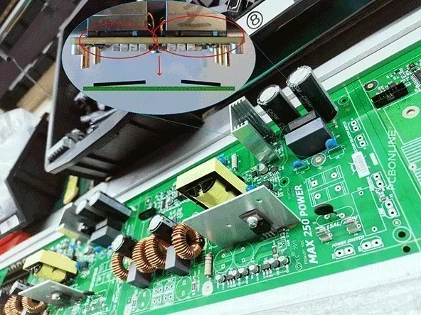
Part 8: Through-Hole and Wave Soldering in GPU PCB Assembly
While most GPU-related components are surface-mount devices, the GPU PCB may still include power connectors, sockets, and large inductors that require through-hole and wave soldering.
Although wave soldering is not the biggest challenge in GPU PCB assembly, we still engineer it with care.
For wave soldering, wave soldering fixtures are used to ensure solder quality without damaging adjacent fine-pitch SMT components. PCBONLINE designs and fabricates custom wave soldering fixtures to press down the through-hole component from flipping, further ensuring reliability and efficiency.
Part 9: Ensuring Reliability in GPU PCB Assembly
Even with perfect assembly, a GPU PCBA still needs to be tested for long-term reliability, as under continuous high-power workloads, solder joints, PCB materials, and thermal interfaces are all stressed.
To ensure reliability, PCBONLINE provides:
- Thermal cycling tests to simulate GPU operation.
- 100% functional testing to verify system-level performance.
- Continuous quality control under ISO 9001:2015, IATF 16949, and IPC-A-610 Class 3 standards.
By combining precision GPU PCB assembly with rigorous testing, we guarantee that every GPU PCBA we deliver can withstand 24/7 high-power and high-speed conditions.
Partner with PCBONLINE for Turnkey GPU PCB Assembly
Whether you are designing next-generation GPUs for AI, GPU servers, or refurbishing existing GPUs for extended use, PCBONLINE provides electronics manufacturing services that cover GPU PCB manufacturing, assembly, testing, and reliability assurance.

Founded in 2005, PBONLINE has two large advanced PCB manufacturing bases and one PCB assembly factory.
HDI PCB fabrication with via-in-pad copper filling for GPU designs with 24+ layers.
SMT assembly with fine-pitch BGA placement accuracy.
Custom reflow profiles for warpage-free soldering.
100% X-Ray inspection for void and defect detection.
Functional testing and thermal aging testing for guaranteed reliability.
BGA reballing services and baking for refurbished GPUs, helping clients reduce costs while maintaining quality.
GPU burn-in programming in the Cloud way, manipulated by you, and protecting your intellectual property.
At PCBONLINE, we combine GPU PCB fabrication, assembly, and testing under one roof, making us a trusted partner for GPU hardware developers. We help customers reduce costs while achieving the highest levels of performance and reliability. If you feel interested in GPU PCB/PCBA from PCBONLINE, send your inquiry by email to info@pcbonline.com.
Conclusion
From fine-pitch BGA soldering and warpage control to precise reflow profiles, void minimization, and HDI design, every step in GPU PCB assembly requires the PCBA manufacturer to have rich expertise and comprehensive advanced equipment. If you're developing or refurbishing GPU products, contact PCBONLINE today for one-stop GPU PCB assembly.
PCB assembly at PCBONLINE.pdf


