
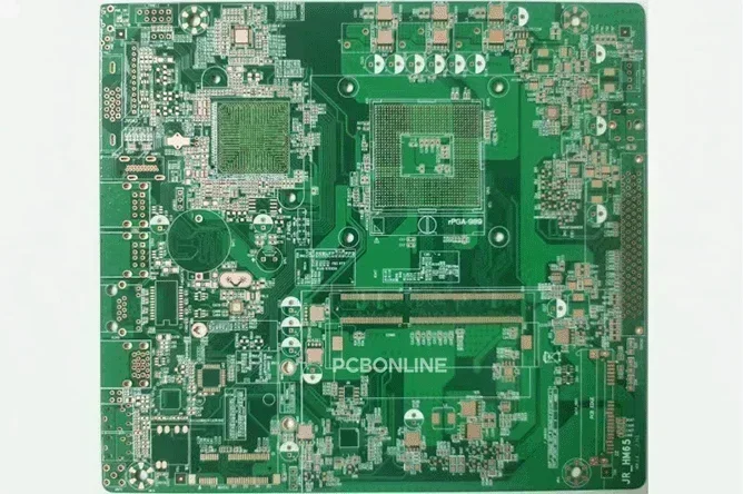
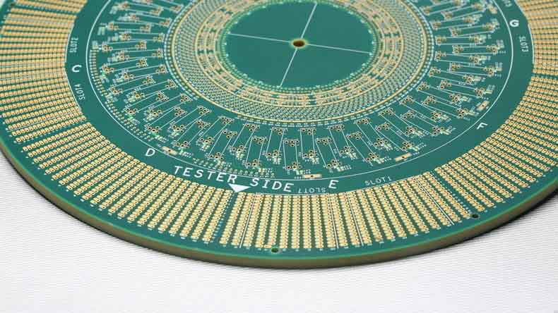
PCBONLINE is a leading high-density interconnect (HDI) PCB manufacturer. We specialize in HDI PCB fabrication and high-reliability circuit board assembly. In this article, we will guide you through the HDI PCB manufacturing process at PCBONLINE step-by-step with pictures taken at our HDI PCB factory.
Overview of HDI PCBs
First, let's understand what an HDI PCB is.
An HDI PCB is a complex printed circuit board featuring sequential lamination, multiple laser drilling cycles up to 8 times, and microvia formation and copper filling.
For example, a 3+N+3 HDI board requires three rounds of laser drilling and lamination
HDI PCBs dramatically reduce device sizes and improve electrical performance. By using PCBONLINE's HDI PCBs in your devices, your application features superior impedance control, high-frequency signal transmission, and enhanced noise rejection.
Our HDI PCBs are ideal for:
- Fine-pitch BGA packages
- Flip-chip assemblies
- Compact high-speed electronic products
Whether you're developing communication electronics, automotive systems, or industrial control devices, PCBONLINE is your reliable partner for HDI PCB manufacturing and one-stop PCB solutions.
HDI PCB Manufacturing Process at PCBONLINE
PCBONLINE has a daily HDI PCB production capacity of 3,000m², and we independently complete every manufacturing step for HDI PCB fabrication.
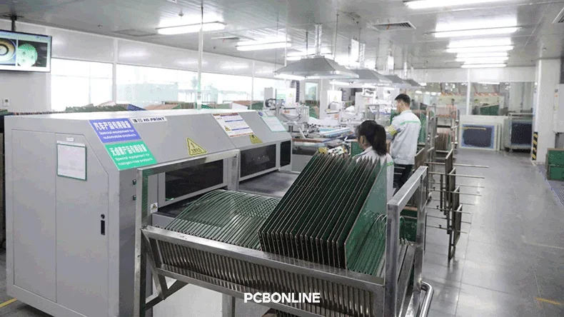
Step 1. Inner and outer layer preparation
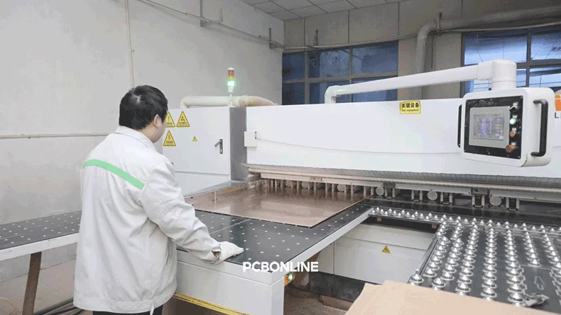
The process starts with automatic blanking. Inner and outer layer materials are cut to the required dimensions. This step sets the foundation for all subsequent manufacturing processes.
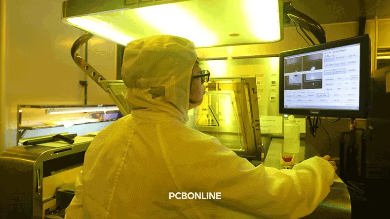
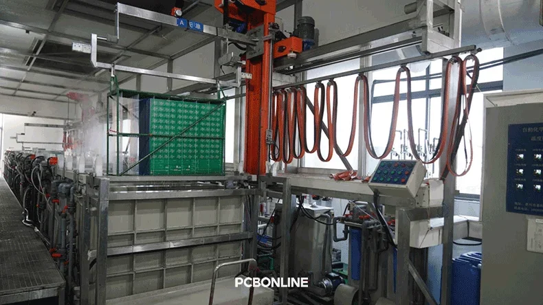
Step 2. Inner layer pre-treatment and imaging
After blanking, the inner layers are automatically cleaned and treated
A photosensitive dry film is then pressed onto the copper laminate.
Circuit patterns are aligned and exposed to UV light, transferring the design onto the film.
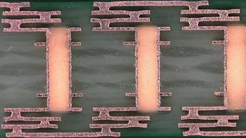
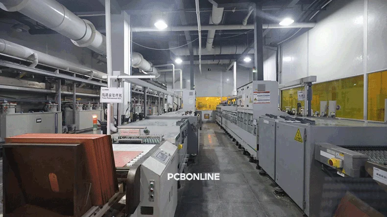
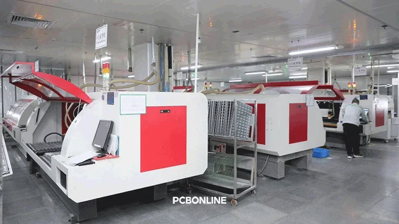
Step 3. Inner layer development, etching, and stripping
Next, the inner layers enter the DES line.
The non-polymerized film is developed and removed.
Unwanted copper is etched away, leaving the circuit traces.
The remaining resist is then stripped off.
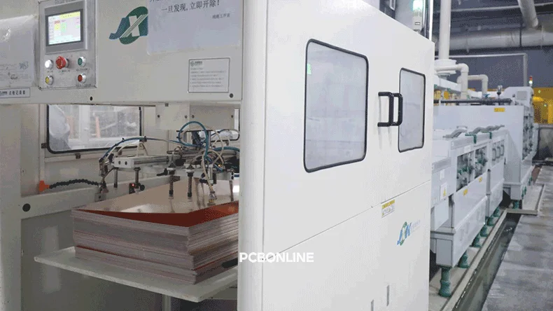
Step 4. Multi-layer lamination
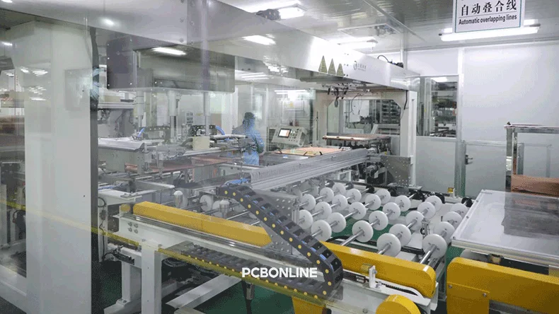
Completed inner layers are stacked with pre-preg and copper foil.
These layers are bonded under high heat and pressure. For HDI PCBs, this lamination is done in cycles.
The browning treatment line ensures strong adhesion between layers.
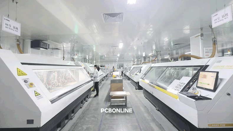
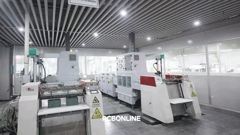
Step 5. Drilling
Drilling creates the holes needed for interconnection. PCBONLINE uses CNC and automatic target drilling machines.
Afterward, deburring removes rough edges. An inspection machine checks the hole quality.
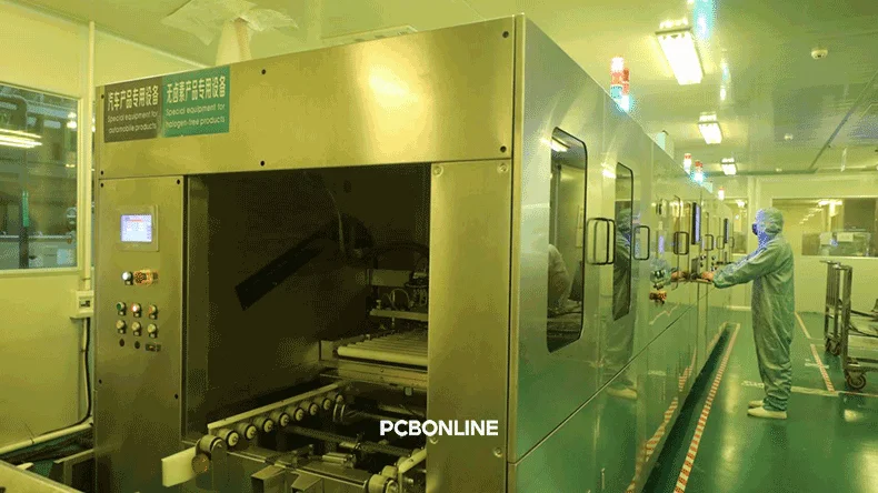
Step 6. Desmear and plating through hole (PTH)
Drilled panels go through Desmear to remove resin.
Then, PTH chemically deposits copper into the holes.
This creates conductive paths between layers.
Step 7. Outer layer pre-treatment and imaging
Outer layers are pre-treated and covered with dry film.
A precise alignment exposure system transfers circuit patterns to the outer layer.
Step 8. Outer layer development, etching, and tin stripping
The outer layers are developed to reveal the circuitry.
Etching removes excess copper.
Tin is then stripped to finalize the outer layer traces.
Step 9. Electroplating
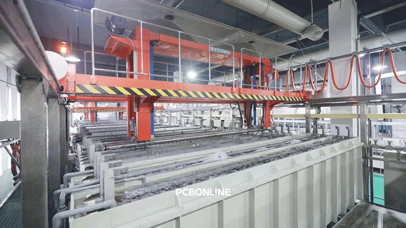
Copper thickness is increased with automatic electroplating.
PCBONLINE uses VCP lines to ensure even deposition on traces and PTH holes.
Step 10. Solder mask application
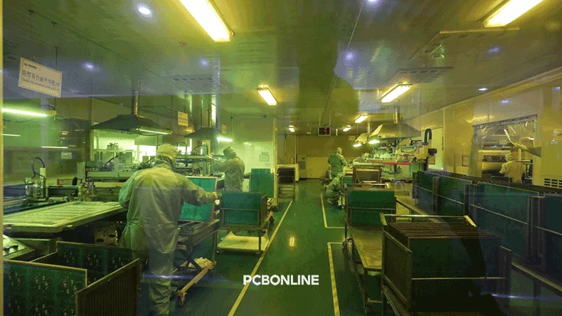
Before applying solder mask, boards may be sandblasted and ground.
The solder mask is printed and exposed with CCD automatic alignment.
Development follows to define mask openings.
Step 11. Silkscreen printing and post-baking
SMD codes, symbols, quality standards, and the logo are screen-printed onto the board.
Post-baking at high temperatures ensures durability.
Step 12. Surface finishing
To protect the copper, surface finishes are applied.
Options include Immersion Gold and HASL. These finishes improve solderability.
Step 13. Final profiling
PCBs are cut from the production panel. This is done using V-CUT and CNC routing based on design requirements.
Step 14. Cleaning and dehumidification
Finished boards are cleaned thoroughly. They undergo dehumidification and leveling. This prepares them for inspection and packaging.
PCBONLINE's Powerful HDI PCB Manufacturing Capabilities
As a specialized HDI PCB manufacturer, PCBONLINE offers powerful capabilities to meet diverse and demanding project requirements. Our expertise allows for custom HDI PCB design and manufacturing with varying copper thicknesses, providing flexibility for different applications.
- Layer count: Support for HDI PCBs ranging from 2 to an impressive 30 layers, accommodating simple to highly complex designs.
- Microvia technology: A minimum laser drill diameter of 0.075mm, enabling extremely fine pitch and high-density interconnects.
- Production capacity: A robust daily production capacity of 3000m², ensuring timely delivery for both small and large-scale orders.
- Advanced stackups: Capability to handle intricate HDI PCB stackups, including 1+N+1, 2+N+2, 3+N+3, and 4+N+4, catering to various complexity levels.
- Diverse via types: Support for a comprehensive range of via types is crucial for HDI designs, such as blind vias, buried vias, staggered vias, stacked vias, and skip vias, providing optimal signal routing and density.
One-Stop HDI PCB Manufacturer from R&D to Fabrication and Assembly
If you plan to develop an HDI PCB or PCBA project and need a turnkey PCB manufacturer with R&D capabilities to ensure the success of your project, you can work with the HDI PCB and PCBA manufacturer PCBONLINE.
Founded in 1999, PCBONLINE has two large advanced PCB manufacturing bases, one PCB assembly factory, stable supply chains, and an R&D team.
PCBONLINE has strong HDI PCB fabrication capabilities, including FR4 HDI PCBs from 4 to 64 layers, HDI flexible PCBs up to 8 layers, HDI rigid-flex PCBs from 4 to 24 layers, and HDI high-frequency PCBs from 4 to 24 layers.
PCBONLINE can meet your HDI PCB demands from the initial idea to high-volume production.
Minimum laser drill: 0.075mm, minimum mechanical drill: 0.15mm
We can make HDI PCBs with structures of 100 µm and 125 µm.
Microvias can be made as single microvias, staggered vias, stacked vias, and skipped vias.
High-density circuit layers up to 20, and microvia PCB layer up to 64.
HDI PCBs 1+N+1, 2+N+2, 3+N+3, and 4+N+4 can be manufactured, and microvias can be in any layer in R&D.
PCBONLINE pays attention to quality and cost-effectiveness in HDI and microvia PCBs. Our engineers with more than 20 years of experience will provide you with one-on-one engineering support throughout the project. If you want to get a quote or ask questions, you can send emails to info@pcbonline.comto get a quote.
Conclusion
PCBONLINE's advanced HDI PCB manufacturing process with cutting-edge equipment and comprehensive quality control paves the way for your project's success. If you need HDI PCBs or have any questions, you can contact PCBONLINE by email or from the table on the right.
PCB fabrication at PCBONLINE.pdf


