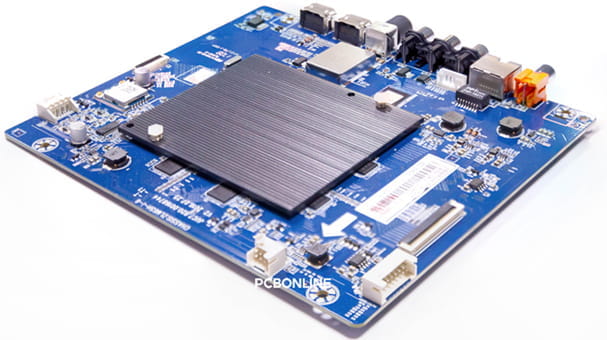
In the electronics manufacturing process, Printed Circuit Board Assembly (PCBA) is critical. During PCB assembly, components are mounted and soldered onto a bare PCB to create a fully functional electronic device.
At PCBONLINE, we provide one-stop PCB assembly manufacturing services, covering everything from prototyping to mass production. Our services include Surface-Mount Technology (SMT), Through-Hole Technology (THT), and even advanced methods such as Chip-on-Board (COB) assembly.
In this article, we will cover an overview of PCB assembly manufacturing, explain the SMT and THT processes in detail, and show how PCBONLINE ensures flawless PCBA production with real-world examples.
Part 1. PCB Assembly Manufacturing Overview
PCB assembly manufacturing involves mounting and soldering electronic components to create working PCBs. The process includes two primary methods:
SMT Assembly (Surface-Mount Technology) – components are mounted directly onto the surface of the PCB.
THT Assembly (Through-Hole Technology) – components are inserted into drilled holes and soldered for strong mechanical bonding.
In addition, PCBONLINE also provides Chip-on-Board (COB) assembly for LED PCBs. COB directly attaches LED dies to the PCB surface and encapsulates them with epoxy. This allows for better thermal management, higher density, and superior light efficiency compared with conventional packaging.
By integrating SMT, THT, and COB, PCBONLINE can meet any PCB assembly requirements for any walk of industries, from consumer electronics to automotive, industrial controls, and aerospace.
Part 2. SMT for PCB Assembly Manufacturing
Surface-Mount Technology (SMT) is the most common method of PCB assembly. Instead of inserting leads into drilled holes, the components for SMT assembly, or SMDs (surface-mounted devices), are placed and soldered directly onto the PCB surface using solder paste and reflow soldering.
SMT allows for high-density designs, faster production, and reduced costs. The typical SMT manufacturing process includes:
- 1. Loading bare PCBs – First, on an SMT line, one of our technicians places the bare PCBs onto the loader one by one, and installs the loader onto the auto-loading machine, which sends the bare PCBs into the next machine - solder paste printer.
- 2. Solder paste printing – In the solder paste printer, an SMT stencil is pre-set with solder paste ready. When a bare PCB is paused beneath the stencil, the solder paste printer's scraper presses the solder paste through the stencil's holes to apply it onto the copper pads of the PCB. Solder paste is a mixture of solder powder and flux, which ensures good wetting and bonding.
- 3. Solder paste inspection (SPI) - The PCB passes the SPI machine, which scans the solder paste position, size, and thickness to ensure its solderability.
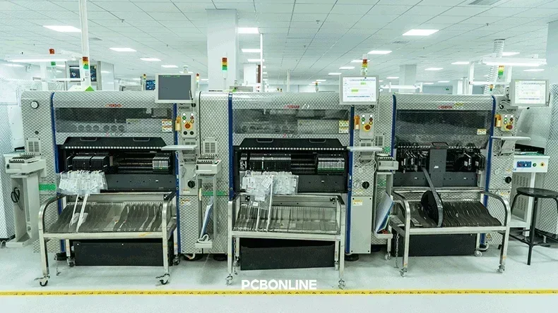
- 4. SMD pick-and-place – At PCBONLINE, each SMT line is equipped with three YAMAHA pick-and-place (PNP) machines. Two high-speed YSM20R machines pick tiny components such as resistors, capacitors, and inductors from the feeders and place them on the PCB. The functional YSM10 machine picks and places larger-footprint components like connectors, buttons, aBGAs, and QFNs onto the paste-covered pads. Our SMT line supports mounting up to 376 SMDs.
- 5. Automated optical inspection (AOI) before reflow – To prevent economic losses, our SMT lines are equipped with a dual-AOI quality control system. Here, our 3D AOI machine scans the SMDs onto the paste-cover pads to make sure no missing or extra components, extra or insufficient solder paste, or any risk of PCB tombstoning.
- 6. Reflow soldering – The PCB then enters a 10-temperature-zone programmable lead-free reflow oven. The solder paste first undergoes a preheat stage, then enters the soak zone, and finally the reflow zone, where it melts and forms permanent electrical and mechanical joints. Controlled cooling prevents thermal stress.
- 7. Automated optical inspection (AOI) after reflow – After reflow, the PCB turns into a PCBA. Our AOI system inspects the PCBA to ensure no solder bridges, misalignments, tombstoning, or insufficient solder.
- 8. X-ray inspection (optional) – Our turnkey PCB assembly factory has two X-ray machines for PCB assembly manufacturing quality control. An X-ray inspection checks the hidden joints of the PCBA to ensure the assembly quality.
- 9. First-article inspection (FAI) – At PCBONLINE, we offer the FAI for PCBA prototyping. Our FAI system generates an inspection report after the inspection for our client to review and decide on mass production.
Below, you can see our PCB assembly manufacturing, including SMT assembly, PTH assembly, post-assembly, material management, and component storage.
Part 3. THT for PCB Assembly Manufacturing
Through-Hole Technology (THT) is another PCB assembly method, especially for components that require strong mechanical support or must handle high currents. In THT, component leads are inserted into drilled holes and soldered either manually or by machine.
A THT assembly process includes:
- Component insertion – Larger or mechanically critical components, such as transformers, connectors, and electrolytic capacitors, are placed into through-holes either by hand or using automated insertion systems.
- Wave soldering – The PCB is passed over a wave of molten solder that simultaneously solders all the PTH component leads. This method is fast and efficient for high-volume assemblies.
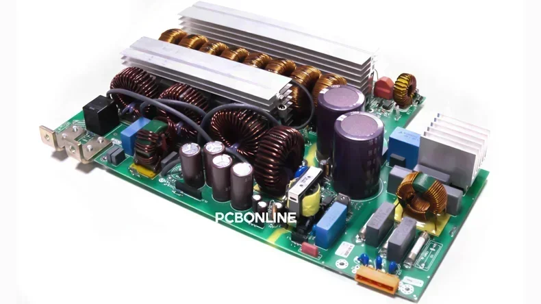
THT remains popular in applications such as power supplies, industrial controls, and automotive electronics, where strength, durability, and current capacity are more critical than miniaturization.
Part 4. How Do We Prevent and Solve Issues in PCB Assembly Manufacturing? – Examples
At PCBONLINE, we recognize that issues in PCB assembly manufacturing can be avoided by DFM and our engineering. That’s why we offer free DFM and engineering and implement proactive measures before PCB assembly manufacturing. Our solutions follow three approaches:
- Fixture design – We design professional fixtures to prevent component shifting, floating, or misalignment during assembly.
- PCB design optimization suggestions – We provide feedback to clients on small PCB layout adjustments to improve manufacturability without affecting functionality.
- Alternative assembly processes – When necessary, we adapt our production lines to use specialized equipment, such as a selective soldering oven, that meets unique requirements, such as soldering sensitive through-hole components easy to damage during wave soldering.
Example 1: Nitrogen reflow for sensitive double-sided PCBs
For double-sided PCBs or assemblies with oxidation-prone and heat-sensitive components, standard reflow soldering can be challenging for them. Oxygen in the environment may oxidize component leads or solder paste, leading to weak solder joints.
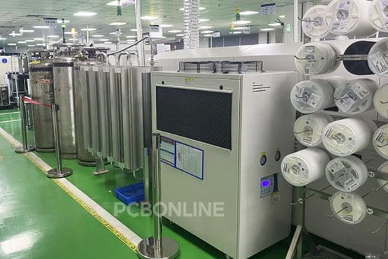
At PCBONLINE, we can use nitrogen reflow soldering. The nitrogen reflow oven creates an oxygen-free atmosphere, the solder flows more smoothly, and forms joints with higher reliability. This process is important for PCBs that use silver-plated pads or contain components such as MOSFETs and RF chips, where solder integrity directly affects performance.
Example 2: Preventing through-hole component floatation
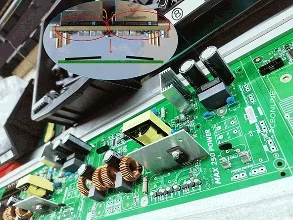
During wave soldering, some through-hole components may float upward due to buoyancy forces in the molten solder wave. This is common with lightweight or long-leaded components. To prevent this, PCBONLINE employs several strategies:
- Custom fixture design – Fixtures press down on components prone to floating, ensuring they remain in position until the solder solidifies.
- Adhesive application – In some cases, we advise our clients to add adhesive beneath components to hold them in place during soldering.
- Selective soldering – Instead of exposing the whole board to a solder wave, selective soldering allows us to precisely solder only the target joints. This method avoids floatation issues and improves consistency.
Example 3: EMI shield design improvement
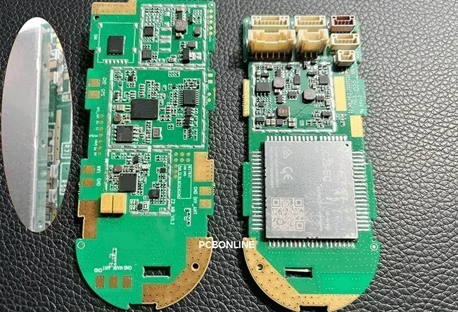
Electromagnetic interference (EMI) is a common concern in high-frequency circuits. In one real project involving an IoT scooter motherboard, EMI noise was affecting communication reliability. Our engineers provided a DFM improvement to the EMI shield design, suggesting adjustments in the shield coverage and grounding points.
By replacing the shielding dome cover with a snap latch design during our DFM review, we allowed the AOI for components beneath the EMI shield and prevented costly post-production modifications.
By applying these strategies, PCBONLINE ensures that our clients’ PCB assembly projects run smoothly, reducing risks and maximizing yield.
Part 5. Partner with PCBONLINE for PCB Assembly Manufacturing
Choose PCBONLINE as your PCB assembly partner from prototypes to mass production. Our PCB assembly manufacturing services offer:
- Turnkey PCB assembly manufacturing – From PCB fabrication, component sourcing, and assembly to testing and shipping.
- DFM expertise – Free DFM checks to identify risks before production begins.
- Professional fixture design – Ensuring stable and reliable assembly.
- Alternative solutions – Such as nitrogen reflow, selective soldering, and COB assembly to meet unique requirements.
- Quality assurance IPC-A-610 Class 3, automotive-grade, or industrial-grade inspection standards.
Founded in 2005, our two advanced PCB manufacturing bases are in Jiangsu and Jiangxi Provinces, and our turnkey PCB assembly factory is in Shenzhen. Besides, we have an R&D team and a global supply network. We also keep strategic cooperation with the top 3 fixture and enclosure manufacturers in China to manufacture the custom PCBA fixtures and device enclosures.
PCBONLINE manufactures, assembles, and tests PCBs and PCBAs to box builds as a source factory manufacturer under one roof, from prototypes to bulky production, saving costs and time for you.
As a source factory for PCBA, our PCB assembly manufacturing is at competitive costs and focuses on PCBA for mid to high-end applications.
Besides SMT and THT assembly, we offer value-added services in the post-assembly stage, including functional testing, IC programming, conformal coating, aging testing, and box-build assembly.
Our high-quality PCB assembly manufacturing is certified with ISO 9001:2015, ISO 14001:2015, IATF 16949:2016, RoHS, REACH, UL, and IPC-A-610 Class 2/3.
Our one-on-one free and professional DFM helps you debug and improve design, to ensure the manufacturability, cost-effectiveness, and final device success.
Whether you need PCB assembly manufacturing for consumer IoT devices, creative electronic products, medical-grade products, etc, we ensure that both PCBA performance and final product presentation meet the highest standards. To get a quote for your PCBA project, email us at info@pcbonline.com.
Conclusion
From PCB fabrication to fully packaged products, PCBONLINE ensures that your electronics are built, assembled, and delivered with precision and care. Our electronics box build services bridge the gap between a finished circuit board and a product your customers can unbox and use immediately.
PCB assembly at PCBONLINE.pdf


