
Aluminum nitride is the most commonly used substrate material for ceramic PCBs (printed circuit boards). If you're developing power electronics, high-brightness LED modules, electric vehicle inverters, or high-frequency RF systems, AlN PCBs are perhaps the best option for PCBs. Aluminum nitride PCBs meet the increasing power density, heat generation, and high-frequency performance requirements, proving reliability and efficiency.
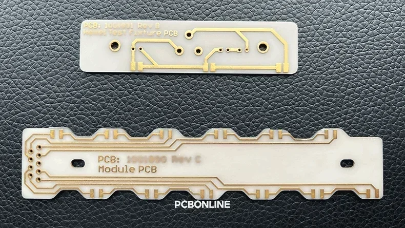
PCBONLINE, a turnkey high-power PCB manufacturer, provides various ceramic PCB manufacturing, including AlN PCBs made in the DPC, DBC, or LTCC technology, customized to meet your project demands.
AlN PCB vs Alumina PCB vs Si₃N₄ PCB vs BeO PCB
The ceramic PCB substrate materials include alumina (aluminum oxide, Al₂O₃), AlN (aluminum nitride), silicon nitride (Si₃N₄), and beryllium oxide (BeO). Among all the ceramic PCBs, why is the AlN PCB the most popular for engineers? AlN PCBs offer the best performance per dollar.
From the comparison below of the four major ceramic PCB substrates, you can understand why AlN PCBs are used the most.
|
Feature
|
AlN
|
Al₂O₃
|
Si₃N₄
|
BeO
|
|
Thermal conductivity (W/m·K)
|
170–200
|
20–35
|
70–90
|
200–260
|
|
CTE (×10⁻⁶/K)
|
4.3
|
7.5
|
3.0
|
7.7
|
|
Electrical properties
|
Excellent RF performance, low loss tangent
|
Moderate RF performance
|
Strong in power but less ideal for RF
|
Good RF, but rarely used due to toxicity
|
|
Mechanical properties
|
High mechanical strength but more brittle than Si₃N₄
|
Robust but weaker than AlN or Si₃N₄
|
Highest toughness and fracture resistance
|
Good strength, but restricted as it is dangerous
|
|
Cost
|
Second heapest
|
Cheapest
|
Second most expensive
|
Most expensive due to safety controls
|
AlN PCB: Thermal Dissipation 170W/m·K to 200W/m·K
AlN PCBs offer high thermal conductivity ranging from 170W/m·K to 200W/m·K. It is 5 to 8 times higher than the thermal conductivity of alumina PCBs, which ranges from 20W/m·K to 35W/m·K.
With the high thermal conductivity, AlN PCBs offer:
- Higher power density for smaller modules with higher continuous output
- Lower operating temperature, reducing thermal stress on sensitive components
- Increased longevity, significantly improving Mean Time Between Failures
- Greater reliability under heavy loads, helping avoid thermal runaway.
The semiconductor junction temperature determines the high-power system's efficiency, long-term stability, and lifetime. AlN PCBs' high conductivity dramatically reduces the thermal resistance between the semiconductor die and the heat sink.
AlN PCBs are ideal for devices such as laser diode modules, IGBT/SiC/GaN power modules, and high-power LEDs.
AlN PCB: CTE Matches with Semiconductor Materials
Thermal expansion mismatch causes solder fatigue, die-attach delamination, and cracking during thermal cycling. The CTE (coefficient of thermal expansion) of AlN PCBs is about 4.3 × 10⁻⁶ /K. It aligns closely with common semiconductor materials:
- Silicon (Si): 3.0 × 10⁻⁶ /K
- Silicon Carbide (SiC): 4.0 × 10⁻⁶ /K
- Gallium Nitride (GaN): 3.3–5.6 × 10⁻⁶ /K
Due to the close CTE with semiconductors, AlN PCBs reduce thermally induced mechanical stress, such as solder joints, die-attach layers, copper metallization, embedded heaters, or sensing elements.
AlN PCBs provide exceptional resistance to thermal fatigue, especially during reflow soldering and repeated power cycling. AlN PCBs offer long-term reliability for automotive power modules, industrial control systems, and high-reliability aerospace electronics.
AlN PCB: Strong RF and High-Frequency Performance
AlN is an excellent material for RF, microwave, and high-speed digital circuits due to a strong balance of thermal, mechanical, and electrical performance. In RF performances, AlN PCBs offer:
- Dielectric constant (εr): 8.8–9.2, lower than Al₂O₃ alumina PCB, enabling faster signal propagation and size reduction.
- Low loss tangent (tan δ): Very low dielectric loss, ideal for GHz-range operation.
- Stable dielectric properties: Minimal variation across temperature and frequency.
AlN PCBs deliver cleaner RF transmission, lower signal attenuation, improved impedance control, better noise immunity, and high-frequency stability. They are popular in radar systems, satellite communications, 5G telecommunications, microwave filters and power amplifiers, and precision sensing and metrology equipment.
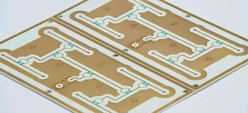
AlN PCB: Compatible with DPC, DBC, AMB, and HTCC Processes
AlN PCBs can be manufactured by the DPC, DBC, AMB, HTCC, or LTCC technology, depending on the requirements of fine lines, high current, and multilayer structures.
DPC is Direct Plated Copper. It enables fine-pitch and high-density routing, achieving line widths/spacing down to 20 μm.
DBC is Direct Bonded Copper, bonding thick copper >200μm directly onto the AlN substrate. It provides strong adhesion and outstanding thermal flow.
AMB is Active Metal Brazing. It provides excellent mechanical and thermal reliability, suitable for ultra-high-power devices requiring thick copper.
HTCC is High-Temperature Co-Ceramic. During the HTCC process, AlN is the main substrate material. HTCC allows advanced multilayer structures and integrates buried components/vias/3D interconnects.
Due to the manufacturing flexibility, AlN PCBs can serve applications ranging from fine-line RF circuits to high-power industrial electronics.
AlN PCB: Cost-Effective and Safe
Though AlN PCBs cost more than alumina PCBs, their performance-to-cost ratio is much higher, especially in thermal performance. Using the AlN substrate, the PCB can use smaller heat sinks, fewer cooling components, higher power density, and lower overall system cost.
Compared with alumina PCBs, AlN PCBs have a higher thermal conductivity, better CTE match with Si/SiC/GaN, and better RF characteristics.
Compared with BeO PCBs, AlN PCBs' thermal performance is similar, but AlN is safe for human beings, while BeO is hazardous to produce and machine.
Compared with silicon nitride PCBs, AlN PCBs are cheaper and have better electrical performance for RF applications.
Applications of AlN PCB
Due to the excellent thermal, mechanical, and electrical properties, AlN PCBs are widely used in high-performance applications.
Power electronics
AlN PCBs' high thermal conductivity and CTE matching significantly enhance reliability under heavy load cycling. They are used for:
- SiC/GaN power modules
- IGBT substrates
- DC/DC and AC/DC converters
- Motor drives and industrial power control
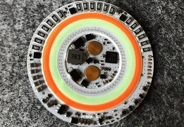
High-power LED and laser systems
The AlN substrate removes heat quickly, prevents wavelength drift, and extends LED/lasing device lifetime. AlN PCBs are used for:
- COB LED substrates
- Laser diode drivers
- Optical amplifiers
RF and microwave systems
AlN PCBs offer stable dielectric properties to ensure clean RF performance. They are used for:
- Power amplifiers
- Low-noise amplifiers
- Filters, couplers, mixers
- 5G and satellite communication modules
Automotive electronics
AlN PCBs support the thermal and mechanical demands of automotive environments. They are used for:
- EV inverter substrates
- On-board chargers
- DC fast-charging power modules
Aerospace and defense
AlN PCBs offer excellent thermal shock resistance and ensure reliability in extreme conditions. They are used for:
- Radar transmit/receive modules
- Avionics power supplies
- Harsh-environment control electronics
Precision sensors and measurement devices
The low dielectric loss and thermal stability of AlN PCBs enable high precision. They are used for:
- Pressure sensors
- Thermal sensors
- High-accuracy analog measurement interfaces
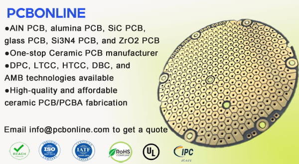
PCBONLINE: High-Quality AlN Ceramic PCB Manufacturer
PCBONLINE is a one-stop ceramic PCB manufacturer founded in 2005, providing turnkey AlN PCB and alumina PCB made by any of the above manufacturing methods. Besides, ceramic IGBT modules, ceramic COB LED modules, ceramic LED plates, etc, can also be provided by PCBONLINE.
PCBONLINE manufactures, assembles, and tests ceramic PCBs as a source factory manufacturer under one roof, from prototypes to bulky production.
PCBONLINE can manufacture ceramic PCBs to be HDI, high-frequency, multilayer, and double-sided.
Provides one-on-one free and professional DFM (design for manufacturing) for ceramic PCB boards before and during prototyping/sampling to ensure the success of your project and seamless mass production.
PCBONLINE has powerful ceramic PCB manufacturing capabilities. The copper layer thickness of ceramic PCBs is arbitrarily customized from 1μm to 1mm.
High-quality ceramic PCB boards with no oxide layer on the PCB surface have better welding performance and high-temperature resistance.
For ceramic PCB manufacturing and assembly orders at $5,000 and above, we offer free complete ceramic PCBA samples and functional tests. If you feel interested in ceramic PCB boards from PCBONLINE, feel free to send your inquiry by email at info@pcbonline.com.
Conclusion
AlN PCBs have excellent performance in thermal management, RF, CTE, electrical properties, and cost-effectiveness, so they are the most used ceramic PCBs. To ensure the success of your AlN PCB/PCBA projects, work with the turnkey ceramic PCB manufacturer PCBONLINE.
PCB assembly at PCBONLINE.pdf
PCB fabrication at PCBONLINE.pdf


