
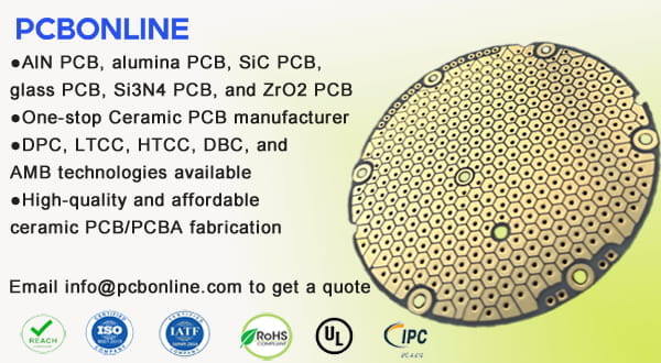
Ceramic substrate printed circuit boards are ceramic PCBs that commonly use aluminum nitride (AlN)or aluminum oxide (Al₂O₃) as the PCB substrate material. Ceramic substrate PCBs feature excellent thermal dissipation, RF performance, profile stability, and chemical resistance. They are used in power devices, automotive sensors, refrigeration devices, etc.
PCBONLINE, a one-stop ceramic PCB manufacturer from prototype PCB to mass PCBA manufacturing, offers aluminum nitride and aluminum oxide substrate PCB manufacturing and assembly. Our ceramic substrate PCBs are 1 to 2-layered AlN or alumina-based based made in DPC (direct plated copper) technology.
Advantages of Ceramic Substrate PCBs
Ceramic substrate PCBs are high-performance and used for high-end applications. They are preferred for high-power and high-frequency devices that require high thermal conductivity due to these advantages.
- Thermal conductivity (λ): Efficiently dissipating heat away from critical components.
- High thermal stability: Withstanding extreme operating temperatures without degradation.
- Low coefficient of thermal expansion (CTE): Closely matching the CTE of silicon chips, reducing thermal stress and increasing reliability.
- High dielectric strength: Ideal for high-voltage applications.

Applications of Ceramic Substrate PCBs
Ceramic substrate PCBs are used in a wide variety of high-performance, high-reliability, and harsh environment applications, meeting the thermal, frequency, or mechanical demands.
Here are the major application fields of ceramic substrate PCBs:
1. High-power and thermal management
Ceramic materials AlN and alumina excel at dissipating heat due to their high thermal conductivity (λ). So they are used in high-power electronics, including:
- LED lighting, especially high-brightness and high-power LED arrays, such as automotive headlights, street lighting, and stadium lights. Ceramic PCBs allow efficient heat removal, which is crucial for LED lifespan and performance.
- Power modules, such as insulated gate bipolar transistor (IGBT) modules, power amplifiers, and solid-state relays. They require ceramic substrate PCBs to handle high currents and massive heat generation.
- Thermoelectric coolers. They use ceramic substrate PCBs to transfer heat efficiently for cooling sensitive components.
- Automotive electronics, including power train control modules and components operating under the hood, where high temperatures are common.
2. High-frequency and RF/microwave systems
Ceramic substrate PCBs have low dielectric loss (loss tangent) and stable dielectric constants (εr), making them ideal for signal integrity at high frequencies for the following high-frequency and RF applications:
- Wireless communication, such as base station amplifiers, antennas, and filters.
- Radar systems, such as high-frequency, high-power radar modules used in defense, aerospace, and automotive safety systems.
- Satellite communications, such as transmitters and receivers, require stable performance in extreme temperature variations.
- RF modules. Ceramic substrate PCBs made by the LTCC (low-temperature co-fired ceramic) technology are used to create compact, integrated RF circuits and SiP (system-in-package) solutions, often embedding passive components (inductors, capacitors).
3. Medical and aerospace/defense
Medical and aerospace/defense electronics for life-critical and mission-critical applications require reliability, airtightness, and stability. Ceramic PCBs meet these requirements and are used for:
- Medical implants, such as pacemakers, defibrillators, and neurostimulators, where a circuit that must be hermetically sealed and highly biocompatible.
- High-reliability sensor systems operating in harsh or high-vacuum environments.
- Aerospace and avionics, such as flight control, navigation, and power distribution. Their circuit requires temperature extremes and radiation stability, which are supported by ceramic substrate PCBs.
- Military and defense, such as high-power jamming systems and secure communication devices.
Ceramic PCBs come in several types, each with distinct manufacturing methods and layer capabilities. Here, we compare the types of DBC/DPC/AMB, LTCC, and HTCC ceramic PCBs.
Ceramic Substrate PCBs: AlN PCB and Alumina PCB
Aluminum nitride (AlN) PCBs and aluminum oxide (Al₂O₃) PCBs are the most widely used ceramic substrate PCBs. Although boron oxide (BeO) has the best high-temperature performance, this ceramic substrate is rarely manufactured because it is toxic and its PCB manufacturing process is dangerous.
Among the two mainstream ceramic substrate PCBs, AlN PCBs offer excellent thermal dissipation, which is 5 to 8 times better than alumina PCBs. AlN PCBs also have advantages over alumina PCBs in high power handling, CTE match to silicon, and better high-frequency performance due to lower dielectric constant and loss tangent.
However, alumina PCBs are cheaper than AlN PCBs. If your project has a limited budget and doesn't require excellent thermal dissipation, you can choose alumina as your ceramic substrate PCB option.
The following details the two mainstream ceramic substrate PCBs.
AlN PCB (aluminum nitride, AlN)
An aluminum Nitride PCB is the premium choice among ceramic substrate PCBs. It is appropriately used for devices demanding the highest level of thermal management.
Characteristics of AlN PCBs are below.
|
Property
|
Value
|
Implications for design
|
|
Thermal conductivity (λ)
|
170W/m·K - 200W/m·K
|
Exceptional thermal dissipation, critical for high-density, high-heat devices.
|
|
Dielectric constant (εr)
|
8.8 - 9.2
|
Lower than Alumina, providing better high-frequency performance.
|
|
Cost
|
High
|
Higher cost than Alumina due to complex processing.
|
|
CTE match
|
Excellent (4.3 x 10⁻⁶)
|
Closely matches Silicon (Si), reducing stress on power chips like IGBTs.
|
Best applications for AlN PCBs include:
- High-brightness/High-power LED arrays
- Power electronics and IGBT modules
- High-frequency radar and satellite communication systems
- Laser diode and thermoelectric cooler heat sinks
Alumina PCBs (aluminum oxide, Al₂O₃)
An alumina PCB is the most cost-effective ceramic substrate PCB.
|
Property
|
Value
|
Implications for design
|
|
Thermal conductivity (λ)
|
20W/m·K - 35W/m·K
|
Good, stable heat dissipation for general power applications.
|
|
Dielectric constant (εr)
|
9.4 - 9.8
|
Suitable for many RF and high-frequency circuits.
|
|
Cost
|
Moderate
|
Most affordable ceramic PCB option.
|
|
Mechanical strength
|
Excellent
|
Mechanically robust and easy to process with standard methods, for example, laser cutting.
|
Best Applications for Alumina PCBs include:
- General-purpose high-power circuits
- Thick and thin-film hybrid circuits
- High-temperature sensors and controls
- LED lighting and automotive electronics, where cost is a major factor
Manufacturing Methods for Ceramic Substrate PCBs
Ceramic PCBs are manufactured using DBC, DPC, thick film, thin film, and co-fired ceramics (HTCC/LTCC) technologies. The choice depends on the required layer count and circuit density.
Direct-bonded copper (DBC)
DBC ceramic substrate PCB manufacturing is a high-temperature eutectic bonding process. Pure copper foil is bonded directly to the ceramic substrate at a temperature near 1065°C in an oxygen-controlled atmosphere. A eutectic liquid Cu₂O forms a strong metallurgical bond.
DBC produces very thick copper layers (100µm to 600µm) with excellent heat transfer.
They are used for high-power modules (IGBTs, MOSFETs) where high current capacity and superior thermal cycling reliability are essential.
Direct-plated copper (DPC)
DPC uses lower processing temperatures (about 300°C) and yields fine line resolution (< 50µm) and high precision.
They are used for high-density circuits, RF components, and semiconductor packaging that require precise alignment and fine features.
Thick film
Thick-film ceramic substrate PCB manufacturing is a screen printing and high-temperature firing process. Conductive, resistive, and dielectric pastes (mixtures of metal powder and glass frit) are sequentially screen-printed onto the ceramic substrate. Each layer is dried and fired at high temperatures (850°C to 1000°C).
The thick film technology allows for the integration of passive components (resistors, conductors) directly on the substrate. The resulting copper thickness is 10µm to 25µm.
They are used for cost-effective mass production of hybrid circuits, sensors, and automotive electronics with moderate precision requirements.
Thin film
Think film ceramic substrate PCB manufacturing is a vacuum deposition and photolithography process. Thin layers of metal, such as Ti, Ni, Au, or Cu, are deposited onto the ceramic surface using high-vacuum techniques like sputtering or evaporation. Precise patterns are then defined using photolithography.
The tin film technology produces the highest precision and finest line resolution (sub-micron) with smooth surfaces. The metal layer is less than 1µm thick before plating.
They are used for high-frequency RF/microwave circuits, precision sensors, and optical applications where surface smoothness and tight tolerances are critical.
Co-fired ceramics (multilayer methods): Co-fired methods are used to create multilayer ceramic PCBs, including multiple circuit layers, vias, and passive components. They include HTCC and LTCC.
High-temperature co-fired ceramic (HTCC)
HTCC ceramic substrate PCB manufacturing is a process of stacking and co-firing at very high temperatures (1500°C to 1800^°C). Layers of ceramic green tape (unfired ceramic) are screen-printed with refractory metal pastes, such as tungsten/W or molybdenum/Mo, for conductors, stacked, laminated, and then sintered into a single piece.
In an HTCC process, the high sintering temperature results in high mechanical strength, excellent chemical stability, and high thermal conductivity (especially with AlN).
They are used for high-power, high-reliability, and harsh-environment applications like hermetic sealing and high-power laser packages.
Low-temperature co-fired ceramic (LTCC)
LTCC ceramic substrate PCB manufacturing is a process of stacking and co-firing at relatively low temperatures (850°C to 1000°C). Layers of ceramic green tape (using glass-ceramic composites) are screen-printed with high-conductivity metals (e.g., Gold/Au or Silver/Ag), stacked, laminated, and sintered.
In an LTCC process, the lower temperature allows the use of highly conductive metal traces, and the process is ideal for embedding passive components (inductors, capacitors) within the layers.
They are used for RF/Microwave modules, wireless communication, and medical electronics requiring high-density, multi-layer integration.
PCBONLINE: High-Quality Ceramic PCB Board Manufacturer
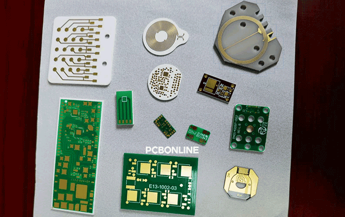
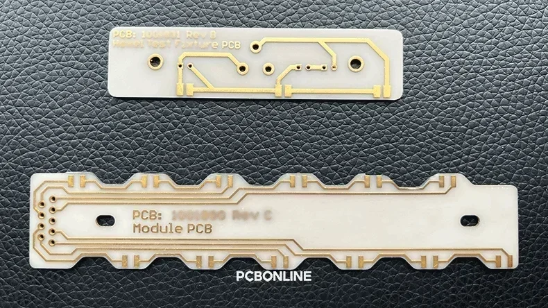
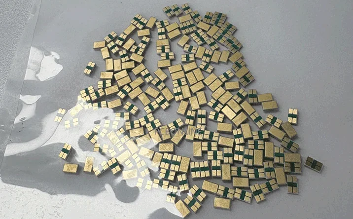
PCBONLINE is a one-stop ceramic PCB board manufacturer founded in 2005, providing turnkey AlN PCB and alumina PCB made by any of the above manufacturing methods. Besides, ceramic IGBT modules, ceramic COB LED modules, ceramic LED plates, etc, can also be provided by PCBONLINE.
PCBONLINE manufactures, assembles, and tests ceramic PCBs as a one-stop source factory, from prototypes to bulk production.
PCBONLINE can manufacture ceramic PCBs to be HDI, high-frequency, multilayer, and double-sided.
Provides one-on-one free and professional DFM (design for manufacturing) for ceramic PCB boards before and during prototyping/sampling to ensure the success of your project and seamless mass production.
PCBONLINE has powerful ceramic PCB manufacturing capabilities. The copper layer thickness of ceramic PCBs is arbitrarily customized from 1μm to 1mm.
High-quality ceramic PCB boards with no oxide layer on the PCB surface have better welding performance and high-temperature resistance.
For ceramic PCB manufacturing and assembly orders at $5,000 and above, we offer free complete ceramic PCBA samples and functional tests. If you feel interested in ceramic PCB boards from PCBONLINE, feel free to send your inquiry by email at info@pcbonline.com.
Conclusion
Ceramic substrate PCBs are mainly AlN PCBs and alumina PCBs, offering high thermal dissipation. To manufacture ceramic substrate PCBs, the methods include DBC, DPC, thick film, thin film, LTCC, and HTCC. To ensure the success of your PCB/PCBA projects, work with the turnkey ceramic PCB manufacturer PCBONLINE.
PCB assembly at PCBONLINE.pdf
PCB fabrication at PCBONLINE.pdf


