
Ceramic-substrate printed circuit boards (PCBs) are used in high-power, RF, high-temperature, and micro-packaged applications due to their superior thermal dissipation, high-frequency performance, dimensional stability, and chemical resistance. In some RF and miniaturization applications, such as RF antennas, implantable medical devices, MEMS pressure sensors, etc, the circuits may require a multilayer PCB design.
How many layers can a ceramic PCB be made to have? Is a four-layer ceramic PCB the limit of multilayer ceramic PCBs? No, four is not the maximum layer number for ceramic PCBs.
If the ceramic PCB manufacturing technology is LTCC (low temperature co-fired ceramic), the PCB can be made to 6- to 12-layer and 20-layer for the limit of mass production.
If the ceramic PCB manufacturing technology is HTCC (high temperature co-fired ceramic), the PCB can be made to 3 to 8 layers.
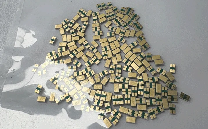
However, for ceramic PCBs manufactured by DBC (direct bonded copper), DPC (direct plated copper), or AMB (active metal brazing) technologies, we can only make them single-layer or two-layer with dual component mounting sides.
Co-Fired Ceramics: Ceramic Multilayer PCB Solution
Co-fired ceramics include LTCC and HTCC, and they are the solutions for ceramic multilayer PCBs. In both methods, several flexible ceramic green tapes are aligned and stacked before sintering. They are then fired together in one high-temperature process, which bonds all the layers into a single, solid multilayer ceramic substrate.
Co-fired ceramics technology completely bypasses the lamination headache by changing the material’s state during the manufacturing process. Instead of stacking already hard ceramic layers, the co-fired ceramics technologies stack flexible and unfired ceramic green tapes before sintering, so multilayer layers can be achieved.
Low-temperature co-fired ceramic (LTCC)
Low-Temperature Co-Fired Ceramic (LTCC) uses a relatively low firing temperature, usually below 1000°C. It can easily support multilayer PCB structures with 6 to 12 layers.
A major advantage of LTCC is that the low sintering temperature allows the use of highly conductive metals such as silver (Ag) or gold (Au) for circuit traces. For this reason, LTCC ceramic PCBs can be used for high-frequency RF, microwave, and millimeter-wave applications.
Besides, LTCC ceramic multilayer PCBs are used in wireless communication modules, sensors, medical devices, and defense systems.
High-Temperature Co-Fired Ceramic (HTCC)
High-Temperature Co-Fired Ceramic (HTCC), on the other hand, is fired at much higher temperatures, typically between 1500°C and 1800°C. HTCC ceramic multilayer PCBs usually contain 3 to 8 layers.
The high processing temperature enables the use of refractory metals like tungsten (W) or molybdenum (Mo) for the traces. It provides excellent robustness and high-power handling capability.
As a result, HTCC offers outstanding mechanical strength and superior thermal conductivity. So HTCC ceramic multilayer PCBs can be used in high-power modules, LED arrays, automotive electronics, and hermetically sealed packages.
Comparison between Different Ceramic PCBs Regarding Layers
Ceramic PCBs come in several types, each with distinct manufacturing methods and layer capabilities. Here, we compare the types of DBC/DPC/AMB, LTCC, and HTCC ceramic PCBs.
DBC/DPC/AMB ceramic PCBs: 1 to 2 layers
DBC, DPC, and AMB ceramic PCBs are used for high-power applications. They usually have one or two copper layers.
DBC/DPC/AMB ceramic PCB structure is simple: a ceramic substrate such as aluminum oxide (Al₂O₃) or aluminum nitride (AlN) is bonded to one or two metal layers, forming a metal-ceramic-metal sandwich. Besides, they don't support via drilling.
Due to their exceptional thermal conductivity and reliability, DBC/DPC/AMB ceramic PCBs are widely used in power electronics, such as IGBT and MOSFET modules, high-power LEDs, and DC/DC converters. However, they are not suitable for complex multilayer routing or miniaturized high-density circuits.
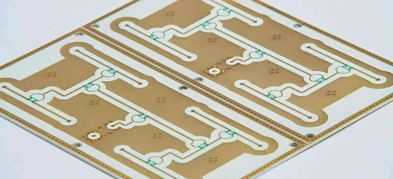
LTCC ceramic multilayer PCBs: 6 to 12 layers
LTCC ceramic PCBs allow multilayer PCB design and are commonly used in RF, microwave, and miniaturized high-frequency applications. They have 6 to 12 layers, and in the limit, can reach 20 layers or even more.
LTCC ceramic PCBs are made by printing conductive, resistive, or dielectric pastes onto thin ceramic green sheets, stacking them, pressing them together, and co-firing at about 850°C.
LTCC allows the creation of through, buried, and blind vias, making it possible to achieve high-density, multilayer circuits.
HTCC ceramic multilayer PCBs: 3 to 8 layers
HTCC ceramic PCBs bridge the gap between multilayer capability and high-temperature performance. They have 3 to 8 layers, with 10 layers being the limit in special cases. Besides, they can accommodate through, buried, and blind vias.
HTCC uses similar stacking techniques as LTCC, but the firing temperature is much higher, around 1600°C.
For a straightforward comparison, there's a table.
|
Technology
|
Ceramic PCB layer
|
Limit layer
|
Via drilling
|
Application
|
|
DBC/DPC/AMB
|
1-2
|
3
|
No
|
High-power, like IGBT and MOSFET
|
|
LTCC
|
6-12
|
20
|
Yes
|
RF, antenna, microwave, sensor
|
|
HTCC
|
3-8
|
10
|
Yes
|
Military, aerospace
|
PCBONLINE: High-Quality Ceramic PCB Board Manufacturer
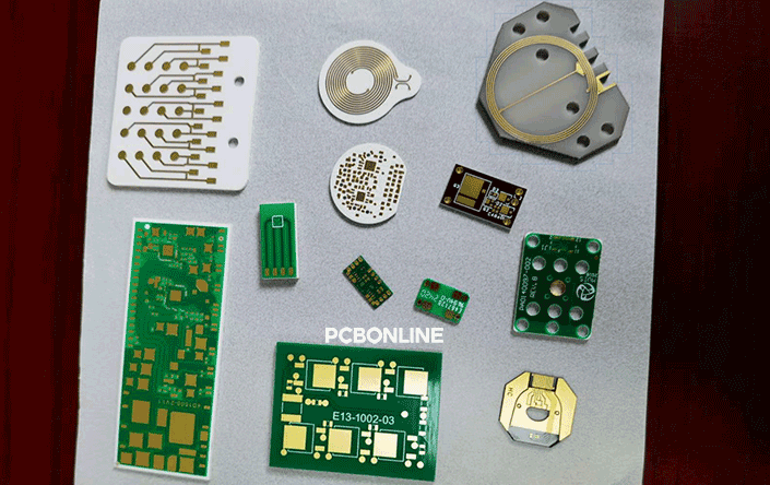
PCBONLINE is a one-stop ceramic PCB board manufacturer founded in 2005, providing turnkey AlN PCB and alumina PCB made by any of the above manufacturing methods. Besides, ceramic IGBT modules, ceramic COB LED modules, ceramic LED plates, etc, can also be provided by PCBONLINE.
PCBONLINE manufactures, assembles, and tests ceramic PCBs as a source factory manufacturer under one roof, from prototypes to bulk production.
PCBONLINE can manufacture ceramic PCBs to be HDI, high-frequency, multilayer, and double-sided.
Provides one-on-one free and professional DFM (design for manufacturing) for ceramic PCB boards before and during prototyping/sampling to ensure the success of your project and seamless mass production.
PCBONLINE has powerful ceramic PCB manufacturing capabilities. The copper layer thickness of ceramic PCBs is arbitrarily customized from 1μm to 1mm.
High-quality ceramic PCB boards with no oxide layer on the PCB surface have better welding performance and high-temperature resistance.
For ceramic PCB manufacturing and assembly orders at $5,000 and above, we offer free complete ceramic PCBA samples and functional tests. If you feel interested in ceramic PCB boards from PCBONLINE, feel free to send your inquiry by email at info@pcbonline.com.
Conclusion
Multilayer ceramic PCBs are made by HTCC or LTCC technologies, and can be 6-12 layers and 3-8 layers, respectively. To manufacture ceramic PCB boards, the methods include thick film, thin film, DPC, LTCC, HTCC, DBC, and AMB. To ensure the success of your PCB/PCBA projects, work with the turnkey ceramic PCB manufacturer PCBONLINE.
PCB assembly at PCBONLINE.pdf
PCB fabrication at PCBONLINE.pdf


