
PCBONLINE is a leading turnkey PCB (printed circuit board) manufacturer for clients around the globe from all walks of industry. We offer comprehensive turnkey PCB manufacturing, from PCB prototypes to massive PCBA box-build assembly. Our turnkey PCB and PCBA factories/production lines/machines are complete and automated. We ensure high-quality electronics production throughout the turnkey PCB manufacturing process.
PCB Manufacturing Process at PCBONLINE
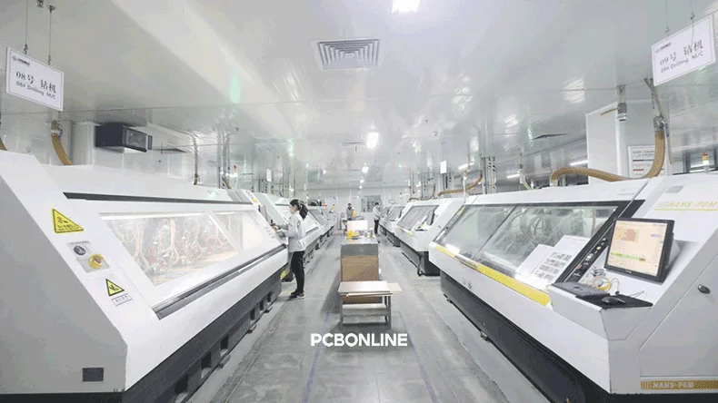
The advanced PCB manufacturing process at PCBONLINE in this article is conducted in our PCB manufacturing bases in Jiangsu Province. It involves multiple stages. Each stage has strict quality control.
Inner layer fabrication
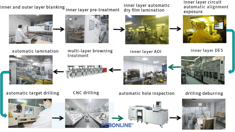
The turnkey PCB manufacturing process starts with material preparation. Inner and outer layers undergo automatic blanking. This prepares the base material.
Next is the inner layer pre-treatment. This cleans the surfaces.
Automatic dry film pressing follows. A photosensitive film is applied.
Inner layer circuit automatic alignment exposure occurs next. This transfers the circuit pattern.
Inner layer circuits then go through an automatic DES line. DES stands for Develop, Etch, Strip. This removes unwanted copper.
Then, an AOI (automated optical inspection) machine checks the inner layer circuit.
Lamination and drilling
After inner layer processing, automatic lamination and pressing begins. A multi-layer browning treatment automatic line is used. This prepares surfaces for bonding.
Multiple layers are bonded together.
Automatic targeting ensures precision drilling.
CNC drilling machines then create holes.
An automatic hole inspection machine verifies drill accuracy.
Drilling deburring removes excess material.
Plating and outer layer processing
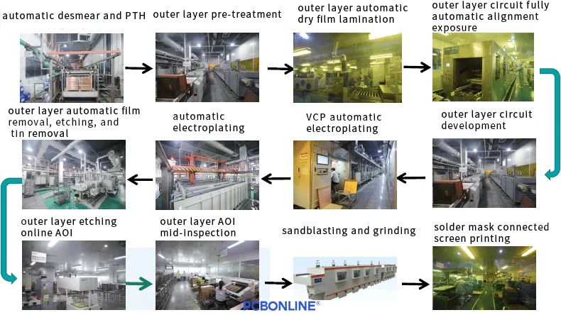
Automatic DSM and PTH (Plating Through Hole) processes add copper to the drilled holes. This creates electrical connections.
The outer layer receives pre-treatment. This cleans the surface.
Outer layer automatic dry film pressing applies a photosensitive film.
Outer layer circuit fully automatic alignment exposure defines the outer layer circuitry.
Outer layer circuit development then removes unwanted film.
VCP automatic electroplating lines are also utilized.
Automatic electroplating lines add copper thickness. Outer layer automatic film removal, etching, and tin removal follow. This defines the copper traces.
Outer layer etching online AOI automatic line inspects etched patterns.
Outer layer AOI mid-inspection is performed.
Solder mask application and finishing
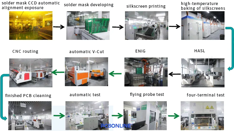
Sandblasting and grinding machines prepare the surface.
The solder mask is then applied in the solder mask connected screen printing workshop.
Solder mask CCD automatic alignment exposure precisely aligns the mask.
Solder mask development completes this step.
Silkscreen printing applies the markings on the PCB.
High-temperature post-baking cures these silkscreen markings.
HASL pre- and post-treatment and immersion gold lines apply surface finishes. These finishes protect the PCB copper pads.
Automatic V-CUT and CNC routing separate the PCB boards in the same panel.
Finished PCBs are cleaned.
Testing and Quality control
In the automated test workshop, the PCBs are checked by automated testes.
The flying probe test ensures no open or short circuits.
PCBONLINE is an advanced turnkey PCB manufacturer. If we work on an automated, medical, aerospace, or military-grade PCB projetc, we have a four-terminal sensing test to ensure the micro resistance in the PCB within the tolerance.

The finished PCBs are dehumidified and leveled.
Finished PCBs undergo automatic AVI (automated visual inspection).
FQC (final quality control) and FQA (final quality assurance) ensure final product quality.
Full size measurement verifies dimensions.
The impedance measurement ensure the PCB impedance within the tolerance for signal integrity.
RoHS (restriction of hazardous substances) detection ensures RoHS compliance.
Metallographic section observation checks internal structure.
Gold, nickel, tin, and REACH detection are performed.
Ionic contamination detection checks cleanliness.
Withstand voltage tests ensure electrical integrity.
Then the PCBs are packaged.
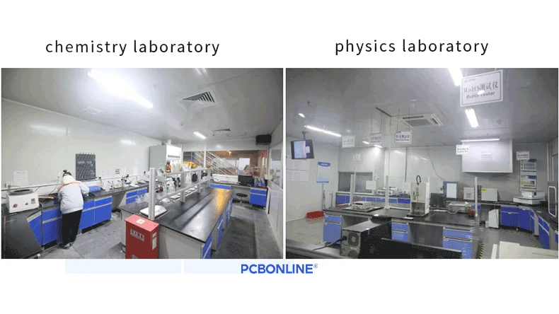
Our physical and chemical laboratories support the above tests. They have advanced equipment, including RoHS testers. Other testing equipment includes test machines, VRS, plating thickness testers, and X-ray machines.
PCBA and Box-Build Assembly Services
PCBONLINE not only provides PCB fabrication. In our turnkey PCB assembly factory in Shenzhen, we offer PCB assembly (including SMT and THT assembly) and box-build assembly.
We handle the entire PCBA and box-build production process, from component procurement, PCB assembly, to enclosures and final product packaging.
As a turnkey PCB manufacturer, our PCB assembly factory in equipped with 4 SMT lines and 4 THT lines, meeting both small-batch and massive PCB assembly neeeds.
SMT assembly
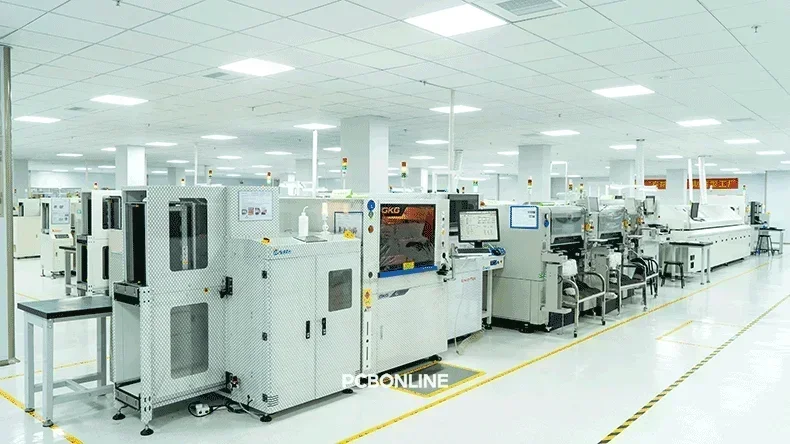
PCBONLINE operates four automated SMT (surface mount technology) lines, each supporting the surface mounting of 376 SMDs (surface mounted devices).
Each of our SMT assembly lines features a 3D SPI (solder paste inspection), two high-speed PNP (pick-and-place) machines, one functional PNP machine, and a dual-AOI system.
The SMT assembly process begins with solder paste printing. Bare PCB boards are placed onto a loader.
Solder paste is applied through an SMT stencil in the solder paste printer.
After printing, the PCB undergoes solder paste inspection to verify the solder paste's position, size, and thickness.
Our two high-speed PNP machines in the YAMAHA YSM20R model mount components in small footprints like 0204 and 0306 resistors and capacitors. They can mount up to 280 SMDs.
A functional PNP machine in the YAMAHA YSM10 model mount larger components, such as MCUs, BGAs, connectors, sockets, and buttons. It supports up to 96 SMDs.
Before reflow soldering, a pre-reflow AOI ensures accurate component placement. This minimizes solder defect risks.
The PCBA then enters a lead-free reflow soldering oven. The solder, SMD, and copper pad form a reliable joint.
A post-reflow AOI inspection is performed afterwards. This ensures soldering quality. It checks for issues like solder bridging, tombstoning, cold soldering, or missing solder.
For PCBA projects involving hidden-joint components like BGA, we conduct an X-ray inspection after SMT assembly. This ensures reliable surface mounting.
After PCB prototype assembly, PCBONLINE performs a first-article inspection (FAI). It ensures functional and mechanical soundness before mass production.
Through-hole THT assembly
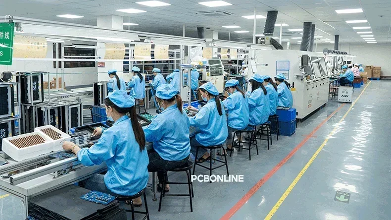
For PCBs requiring THT assembly, PCBONLINE offers efficient assembly using THT or DIP lines. These lines are semi-automated. They involve inserting THT component leads through PCB holes and then wave soldering.
PCBONLINE designs wave soldering fixtures. These protect the PCBA from high temperatures. They also press down components prone to floating during soldering.
After wave soldering, THT component leads on the underside are trimmed to one to two millimeters and touched-up for soldering optimization.
In post-assembly, we debug the PCBA and has an visual inspection to ensure quality. PCBONLINE also offers value-added services, including IC programming, burn-in tests, conformal coating, and PCBA functional tests.
Box-build assembly
PCBONLINE maintains long-term cooperation with the top 3 enclosure/mold manufacturers in China for manufacturing of the enclosures and molds.
At PCBONLINE's turnkey PCB factory, we install the enclosure onto the PCBA to create the final box-build devices.
Afterward, we perform an application simulation test to ensure all mechanical, electrical, and aesthetic requirements of the final products are met in uses.
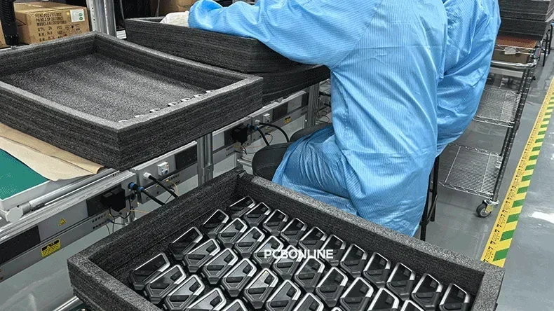
Then we label and package the box-builds to be the finished devices, which are ready to deliver to our clients.
When our client approves the box-build sample, we will put into massive production.
Material management and Certifications
Turnkey PCB manufacturing requires efficient and clear material management to support one-stop fabrication. Besides, as turnkey PCB manufacturing produces the finished devices, the turnkey PCB manufacturer should meet industry standards.
Component and material management
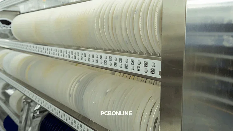
PCBONLINE prioritizes robust component management. Components undergo X-ray inspection before storage and use. We use smart shelves to place components. Every time we put in or take out, we have to scan the QR code to register in the warehouse. For active and high-value components, we store and manage them in temperature- and humidity-controlled cabinets.
SMT stencils from previous projects are stored for reorders. And we carefully manage solder paste in a smart solder paste cabinet. They maintain stable supply chains. They collaborate with top fixture and enclosure manufacturers.
Certifications

PCBONLINE's turnkey PCB manufacturing meets high industry standards, are certified with ISO 9001:2015 and ISO 14001:2015. Our IATF 16949:2016 certification demonstrates automotive industry compliance. We also adhere to RoHS and REACH directives. And UL and IPC-A-610 Class 2/3 certifications further highlight our quality.
Partner with PCBONLINE for Turnkey PCB Manufacturing
With 20 years of expertise, advanced manufacturing facilities, and strict quality control, PCBONLINE is a reliable PCBA manufacturer for turnkey PCB manufacturing.
Founded in 2005, PCBONLINE has two advanced PCB manufacturing bases in Jiangsu and Jiangxi Provinces, one turnkey PCB assembly factory in Shenzhen for PCBA and box builds. We also have an R&D team.
We provids one-on-one free and professional DFM before and during prototyping/sampling, to ensure the manufacturability and project success.
The professionals at PCBONLINE design the PCBA fixtures and manufacturing molds that accurately fit the PCBA manufacturing and test processes.
Complete equipment and capabilities for turnkey PCB manufacturing, including PCB manufacturing, PCB assembly, value-added (such as functional test, IC programming, and burn-in test), and box-build assembly.
PCBONLINE manufactures, assembles, and tests from PCBs and PCBAs to box builds as a source factory manufacturer under one roof, from prototypes to bulky production, saving costs and time for you.
High-quality PCBA manufacturing certified with ISO 9001:2015, ISO 14001:2015, IATF 16949:2016, RoHS, REACH, UL, and IPC-A-610 Class 2/3.
PCBONLINE can design the test points for your PCB and offer improvement suggestions for your design if there needs any optimization.
When your turnkey PCB project enters mass production, we refund the fees of prototypes and offer free PCBA functional testing.
Whether you need prototype assembly, PCB low-volume runs, or high-volume box build production, we have the equipment, experience, and capabilities to deliver superior results. To get a quote for turnkey PCB manufacturing, email us at info@pcbonline.com.
Conclusion
Turnkey PCB manufacturing includes everything from PCB fabrication, PCB assembly, to box-build assembly. PCBONLINE provides high-quality turnkey PCB manufacturing. To ensure the manufacturing success of your project, partner with the turnkey PCB manufacturer PCBONLINE.
PCB assembly at PCBONLINE.pdf


